CPUs (Microprocessors)
One of the most critical components of a PC is the Central Processing Unit (CPU) - the microprocessor. Until the 3D gaming era, the CPU was what defined the perfomance of your computer. This page takes a look at all the major CPUs used in PCs from 1982 through to 2000. In some cases there were clones or licenced variants - details of these can be found in the relevant section.
To help simplify the huge array of CPUs over the years, they are sometimes put into "generations", like in the table below.
| Gen | Years | CPUs | Socket/Slot |
|---|---|---|---|
| 1 | 1978-1983 | Intel 8088 / 8086, NEC V20/V30 | 40-pin DIP socket |
| 2 | 1984-1986 | Intel 80286, AMD/Harris/Siemens 80286 | 68-pin PGA socket |
| 3 | 1987-1989 | Intel 80386DX, 386SX, AMD Am386, Cyrix Cx486 | 132-pin PGA socket or soldered-in |
| 4 | 1990-1992 | Intel 80486DX / 486SX / 80487 / 486 Overdrive / 486DX2 / 486DX4, AMD Am486, AMD Am486DX2/4, Cyrix Cx486DX2/4, AMD 5x86, Cyrix 5x86 | 168-pin Socket 1, Socket 2 or Socket 3 |
| 5 | 1993-1997 | Intel Pentium (classic), Cyrix 6x86, AMD K5, Intel Pentium Overdrive, IDT WinChip C6 | Socket 4, Socket 5, Socket 7 |
| 5.5 | 1997-1998 | Intel Pentium MMX, Cyrix 6x86MX/MII | Socket 7, Super Socket 7 |
| 6 | 1995-1998 | Intel Pentium Pro / Pentium II, AMD K6/K6-2 | Slot 1, Socket 7, Super Socket 7 |
| 6.5 | 1999 | Intel Celeron / Pentium III, AMD K6-3, VIA C3 | Slot 1, Socket 370, Super Socket 7 |
| 7 | 1999-2000 | AMD Athlon (K7) | Slot A, Socket 462 |
Intel 8086
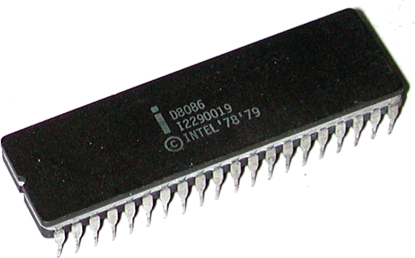 Launched in 1978 after Intel's success with its much earlier 8080 microprocessor, the 8086 was designed to permit assembly language for the 8080 and 8085 to be converted to equivalent 8086 source code. It added new instructions to support signed integers, base+offset addressing, and self-repeating operations. It was created using Intel's new HMOS manufacturing process (High Performance MOS) which was setup to create fast static RAM products. Both internal and external data bus are 16-bits wide, and the 8086 could address up to 1 MB of memory, in 64 KB segments and changing the segment register to look at further 64 KB segments.
The 8086 and 8088 could be used in tandem with a mathematical coprocessor to add hardware/microcode-based floating point performance. The Intel 8087 was the standard math coprocessor for the 8086 and 8088, operating on 80-bit numbers. Manufacturers like Cyrix and Weitek eventually came up with high performance floating point coprocessors that competed with the 8087 as well as with the subsequent, higher performing Intel 80387.
Originally the 8086 was released with a 5 MHz clock speed - this chip was simply branded "8086", but later variants were specified to run at up to 10 MHz. These were branded 8086-1 and 8086-2. The typical unit price of the 8086 was around $200 in 1980. Compatible, and in some cases enhanced versions, were also manufactured by Fujitsu, Harris/Intersil, OKI, Siemens AG, Texas Instruments, NEC, Mitsubishi, and AMD.
The 6 MHz 8086 scores a MIPS (Millions of Instructions Per Second) rating of 0.9.
The 10 MHz 8086 scores a MIPS (Millions of Instructions Per Second) rating of 1.5.
The 12 MHz 8086 scores a MIPS (Millions of Instructions Per Second) rating of 1.8.
The 8086 was available in both ceramic (D) and plastic (P) packages.
An 8086 cannot be replaced with an 8088 due to the differences in their data bus width (16-bit vs 8-bit). The standard "drop-in" upgrade for an 8086 is the NEC V30.
Data sheets: iAPX 86/88 Users Manual (1981), iAPX 86/88/186/188 Users Manual (1985), iAPX 86/88/186/188 Microprocessors Part 1 (Jun 1984), iAPX 86/88/186/188 Microprocessors Part 2 (Jul 1984)
Programming: iAPX 86/88/186/188 Programmers Reference Manual (1983)
Intel 8088
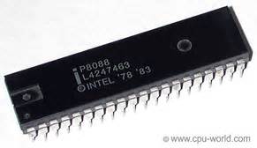 In 1979, a year after the 8086, the 8088 was launched, It was pin-compatible with its older sibling, and had the same architecture internally with the only difference being a narrower external data bus width on the 8088 (8-bit instead the 8086's 16-bit). This means the 8088 required two consecutive bus cycles to read/write 16-bit data instead of one bus cycle for the 8086, making it slower than the 8086 in performing 16-bit tasks. Both CPUs have an identical Execution Unit (EU) - only the Bus Interface Unit (BIU) and the prefetch queue differ (reduced to 4 bytes in the 8088 from the 8086's 6 bytes).
One of the primary reasons for the creation of the 8088 was to add compatibility with the 8080/8085 CPU, so that it would be easy and cheap for new 8088-based computers to make use of the tried and trusted support chips already in use by manufacturers who had knowledge of the 8080 and 8085 CPUs. This was crucial at the time because 8-bit support chips were much cheaper to buy than 16-bit chips, and there was more choice for manufacturers. This is one of the reasons IBM chose the Intel 8088 for its new IBM 5150 computer, coupled with the fact they had already acquired the rights to manufacture the 8086 family of CPUs. Intel offered a lower price to IBM for the 8088 than the 8086.
Early Intel 8088s were manufactured with an interrupt bug, which meant the CPU allowed interrupts to occur after a program changed the stack segment register. Usually an interrupt is not allowed until the instruction after the one that changed the stack segment register. Around 200,000 IBM 5150 PCs left the factory with this defective chip. Those with the defect can be identified easily as they have (C) INTEL 1978 stamped on them. If they have (C) INTEL '78 '81 or (C) INTEL '78 '83, they are later bug-free variants.
![]() The original 1979 production of the 8088 allowed the CPU to be specified to run at a clock speed of 5 MHz, but a later revision, the 8088-2 which used the new nMOS fabrication process allowed the CPU to be specified at up to 8 MHz. Later variants manufactured by third parties like AMD and Harris would be able to realise clock speeds up to 16 MHz and even 20 and 25 MHz. The most common IBM PC-compatibles that used the Intel 8088 ran at 8 MHz or 10 MHz.
The original 1979 production of the 8088 allowed the CPU to be specified to run at a clock speed of 5 MHz, but a later revision, the 8088-2 which used the new nMOS fabrication process allowed the CPU to be specified at up to 8 MHz. Later variants manufactured by third parties like AMD and Harris would be able to realise clock speeds up to 16 MHz and even 20 and 25 MHz. The most common IBM PC-compatibles that used the Intel 8088 ran at 8 MHz or 10 MHz.
![]() For lower power consumption requirements, Intel employed the fully static CHMOS design to create the 80C88 and 80C88A, which permitted the CPU to run anywhere from 0 to 8 MHz, with a "standby" mode.
For lower power consumption requirements, Intel employed the fully static CHMOS design to create the 80C88 and 80C88A, which permitted the CPU to run anywhere from 0 to 8 MHz, with a "standby" mode.
The 8088 can address up to a maximum of 1 MB of memory, and uses the same segmented memory addressing as the 8086. They are both able to address 64 KB of memory directly. Addressing memory beyond this requires the CPU to break up the task into multiple tasks, addressing blocks of 64 KB at a time and moving the segment register on each time (like a pointer).
Like the 8086, the 8088 supports the 8087 floating point co-processor. The prime reason for having a separate co-processor is that the CPU will automatically send all floating-point instructions for processing in parallel by the co-processor, leaving the main CPU to handle other instructions.
Performance of the 8088 is very similar to the 8086, with almost negligible difference, despite the 8086's superior 16-bit external data bus width.
An 8088 cannot be replaced with an 8086 due to the differences in their data bus width (8-bit vs 16-bit). The standard drop-in upgrade for an 8088 is the NEC V20.
Data sheets: iAPX 86/88 Users Manual (1981), iAPX 86/88/186/188 Users Manual (1985), iAPX 86/88/186/188 Microprocessors Part 1 (Jun 1984), iAPX 86/88/186/188 Microprocessors Part 2 (Jul 1984)
Programming: iAPX 86/88/186/188 Programmers Reference Manual (1983)
NEC V20/V30
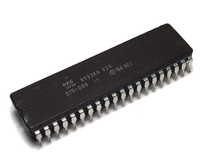 Whilst NEC was an authorised manufacturer of Intel 8088 and 8086 microprocessors (they had part number μPD8088D and μPD8086D respectively), in 1982 NEC also launched enhanced but pin-compatible versions, called the V20 (part number μPD70108) and V30 (part number μPD70116). These incorporated the instruction set of the Intel 80186 CPU (an enhanced 8086 with embedded DMA controller, interrupt controller and more), and some of the speed enhancements of that CPU too, in order to allow computer manufacturers to have an upgrade path without changing their circuit designs. They also contained a special Intel 8080-emulation mode, where instructions could be given to enter emulation mode and execute programs written for the Intel 8080 processors.
These chips tended to run at between 5 and 10 MHz, but at the same clock speed as their respective Intel cousins the NEC chips performed about 30% faster, primarily due to faster effective address calculation along with faster loop counters, shift registers and multiplier. Sony also produced NEC's V20 chip, V20H with part number Sony CXQ70108. The NEC V20 especially was commonplace with PC compatibles, especially "turbo" XT models.
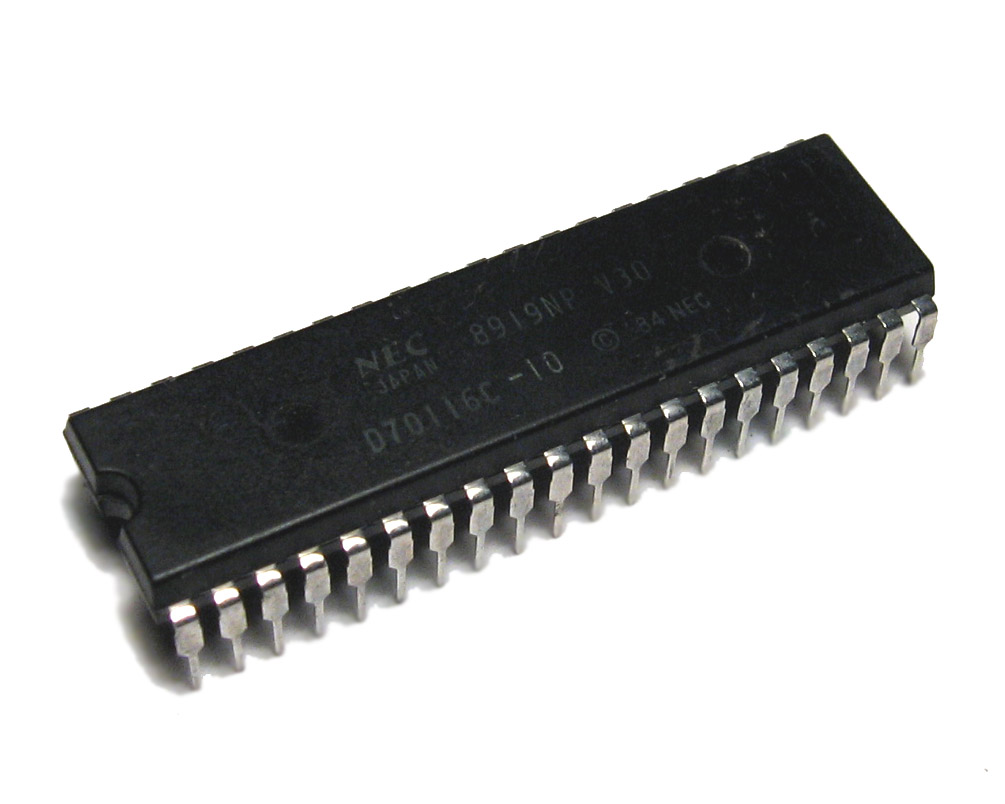 The V30 was a version of the V20 that was pin-compatible with the Intel 8086, as well as having its wider 16-bit data bus. Aside from this difference, it was identical to the V20.
The NEC V20, V30, and Intel's 8088 and 8086, can universally run the same software.
In 1995, NEC enhanced the V20 and V30 with faster execution times and lower power use. These new variants were called V20HL (μPD70108H) and V30HL (μPD70116H). These are available in 10, 12 and 16 MHz versions. I've personally installed an NEC V20H (16 MHz version) into an old XT motherboard as a drop-in replacement for my Sony-branded V20 which ran at 8 MHz, and it works just fine. Of course, its clock speed is controlled by the motherboard, so this new chip ran at 8 MHz also (half its possible clock speed).
I ran the Landmark Speed Test 6.0 utility on an XT-compatible that's designed to run at 8 MHz with a V20H-16 installed. It reported that the computer was running like a 6 MHz AT.
V20 and V30 User Manual
Data sheets: NEC V20HL (μPD70108H)
What Happened to the 80186?
Intel's enhanced 8086 CPU, the 80186, could have been the obvious successor, but it was really designed for embedded solutions.The 80186 had an 8086-compatible CPU core (with more instructions on top), but also had a DMA controller, Peripheral Interrupt Controller, Clock Generator and Programmable Interval Timer all built into the chip. This meant it was cheaper to design a new system using this chip since fewer external components and "glue" logic would be needed.
Unfortunately, none of this additional integrated hardware was compatible with the IBM PC which used a different DMA controller, PIC and PIT on the motherboard, so it was not beneficial to use the 80186 in a PC design. Some PC makers did use the 80186, including the RM Nimbus PC-186, Goupil G4, COMPIS, Tandy 2000, Siemens PC-D and HP's 100LX and 200LX palmtops. These were all mostly PC-compatible though some software would not work unless written specifically to account for the hardware differences.
Intel 80286
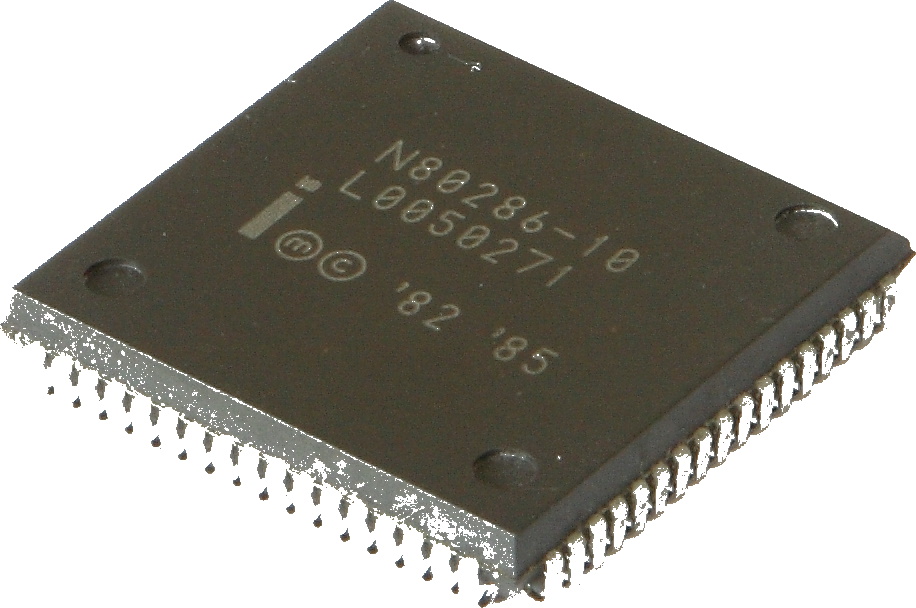 Introduced in February 1982 with IBM PC/AT (Advanced Technology), the Intel 80286 added non-multiplexed address and data buses, but the key differentiator over the 8086/8088 (and the NEC compatibles) was "protected mode". When the CPU was in protected mode, the CPU could address up to 16 MB of memory - well above the 1 MB limit of the 8086/8088. It was called protected mode because it was possible to protect sections of memory and other system resources from user programs - something that was essential for good multitasking. The 80286 started up in what was later called 'Real' mode (meaning every memory address corresponded to a "real" physical memory location), and it was this mode that the 8088/8086 and NEC equivalents only had.
Protected mode was used by OS/2 1.x, Venix, SCO Xenix 286, and other operating systems. Although this feature was great for new operating systems that were designed to use it, running older x86 programs designed for 8086/8088 still meant the 286 was unable to run more than one of these programs at once and make use of this feature. Also, the CPU was unable to reliably switch between 'Real' mode and 'Protected' mode without a system reset. Since DOS was still the de-facto operating system throughout the 286's useful life, protected mode was largely ignored, rendering the 80286 to be nothing more than a "turbocharged 8086/8088".
Whilst protected mode and being able to access up to 16 MB of memory was good, the maximum memory segment size was still the same 64 KB as with the 8086/8088 CPUs.
Clocks speeds for the Intel 80286 ranged from 6 MHz up to 12.5 MHz.
Typically the bus speed was tied to the CPU clock speed, just as with the 8088 and 8086 before it, but in order to achieve clock speeds beyond 10 MHz the bus had to be decoupled from the CPU, since there was no way expansion cards could keep up with the rapidly increasing speeds of the processor. This decoupling meant that the ISA bus could still be driven at a conservative 8 MHz or 10 MHz for stability, while the CPU and other motherboard components would be able to run at the higher clock speed. This was when companies like Chips & Technologies (C&T) entered the market with ASICs that simplified motherboard design and allowed separate control over the CPU clock and the external bus clock.
The 80286 was a major step up from the 8088/8086 in terms of performance at the same clock speed. Norton SI (System Information) benchmarks for the 80286 compared to the 8088 are as follows, showing how much more efficient the 80286 is (about 2.5x):-
| MHz | 4.77 | 6 | 8 | 10 | 12 | 16 | 20 |
|---|---|---|---|---|---|---|---|
| 8088 | 1.0 | 1.3 | 1.7 | 2.1 | |||
| 80286 | - | 3.1 | 4.4 | 5.6 | 6.7 | ~9.0 | ~11.5 |
A math co-processor was also made for the 80286 by Intel, called the 80287.
Data sheets: Introduction to the iAPX 286 (1982), iAPX 286 Hardware Reference Manual (1983), iAPX 286 Operating System Writers Guide (1983), 80286 Hardware Reference Manual (1987),
Programming: iAPX 286 Programmers Reference Manual (1983), iAPX 286 Programmers Reference Manual (1985), 80286 and 80287 Programmers Reference Manual (1987)
Other 80286
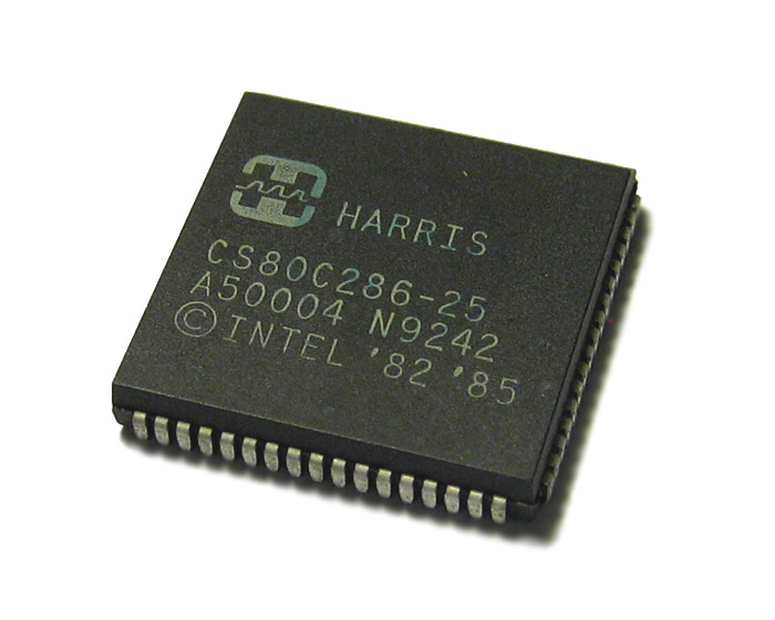 The Intel 80286 was also manufactured by a number of licenced third parties, including Fujitsu (MBL80286), AMD (N80L286), Harris/Intersil (CS80C286/IS80C286), IBM (CG80286), and Siemens. It was always manufactured in a 68-pin PGA package.
With Intel releasing versions from 6 MHz up to 12.5 MHz, these other authorised manufacturers later developed 16, 20 and 25 MHz versions. Around the time we first saw 16 MHz 286s the 80386 was soon to arrive. The primary reason why these third parties continued to develop the 80286 with faster clock speeds was because Intel locked them out of licencing the 80386. By 1988 Intel had moved on and was too busy turning out faster 386s and designing the 486 to spend much time squeezing more out of its old 286 design.
Without the ability to sell the now-current generation CPU (the 386), AMD had taken over the role of supplying most AT compatibles with their processor, but it lacked the resources to further develop the 286 design to run faster and compete with the Intel 386 and 386SX.
Harris Corp., filled the vacuum with a CMOS 286. It was faster, used less power, and generated less heat than Intel's and AMD's 286s. Computer makers pounced. Dell, Northgate, and others introduced new models. In fact, the bumper crop of 1988 and 1989 286-based laptops was, in large part, a direct result of Harris's introduction of a fast CMOS processor. In October 1988, AMD closed one of its factories and laid off 8% of its work force due to declining orders. In November 1988, Harris acquired GE's semiconductor business for $208 million. One of the reasons for the purchase was to increase production lines. At the time, Harris said it was facing "a very significant backlog of orders for the 80C286", and planned to use one of its newly acquired plants in England to boost its 286 production capacity. Several days after this announcement, AMD laid off a further 7% of its work force stating it would switch a plant to CMOS production.
For an in-depth performance review of these faster 286s, head over to my four-part article on getting a 286 to run like a 386.
Intel 80386DX
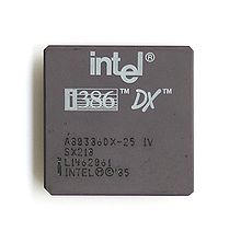 In 1985, Intel introduced the third generation of its 80x86 family - the 80386. This resolved many of the shortcomings of the 80286, with a full 32-bit set of registers and instructions. It also increased the memory segment size from 64 KB to 4 GB, which meant applications didn't need to concern themselves with switching memory segments to read different areas of memory. The new CPU also got a more enhanced protected mode, which was easily switchable back to real mode when required (no more system reboot as with the 80286). Another key backward compatibility boon was the new "virtual 8086" mode, which allowed the 386 to run old 8086/8088 applications whilst providing necessary protection of memory and other resources. This opened the door for multitasking, since the PC could now run multiple "virtual" 8086s all with their own protected memory space.
The 'DX' suffix stood for (Double-word eXternal), indicating the width of the CPU's external data bus interface (32 bits wide external to the CPU's core).
Intel's clock speeds for the 80386 ranged from 16 MHz up to 33 MHz, with this final iteration launched in April 1989 as they shifted focus to the new 80486.
In raw performance, there wasn't much of a difference between an 80286 and an 80386 unless software was written to harness the new features of the 386. Indeed, many 80286 PC manufacturers were touting that their 80286 16 MHz and 20 MHz systems were just as fast as 16 and 20 MHz 386 systems, and they were right! However, when software made use of the 386's extra "modes" and its enhanced memory management unit, performance gains were massive. A 33 MHz 80386 could operate at about 11.4 MIPS, compared to an 80286 @ 12 MHz that clocked in at 2.6 MIPS, or an Intel 8086 @ 10 MHz that could operate at 0.75 MIPS.
| Processor | SpeedSys Score |
|---|---|
| 80386DX-16 | 1.88 |
| 80386DX-20 | 4.10 |
| 80386DX-25 | ? |
| 80386DX-33 | 4.93 |
| 80386DX-40* | 6.37 |
*Not an Intel CPU. This rating is of a Texas Instruments clone.
Data sheets: Introduction to the 80386 (Apr 1986), 80386 Hardware Reference Manual (1986), 80386 Hardware Reference Manual (1987)
Programming: Programmers Reference Manual (1986)
Intel 80386SX
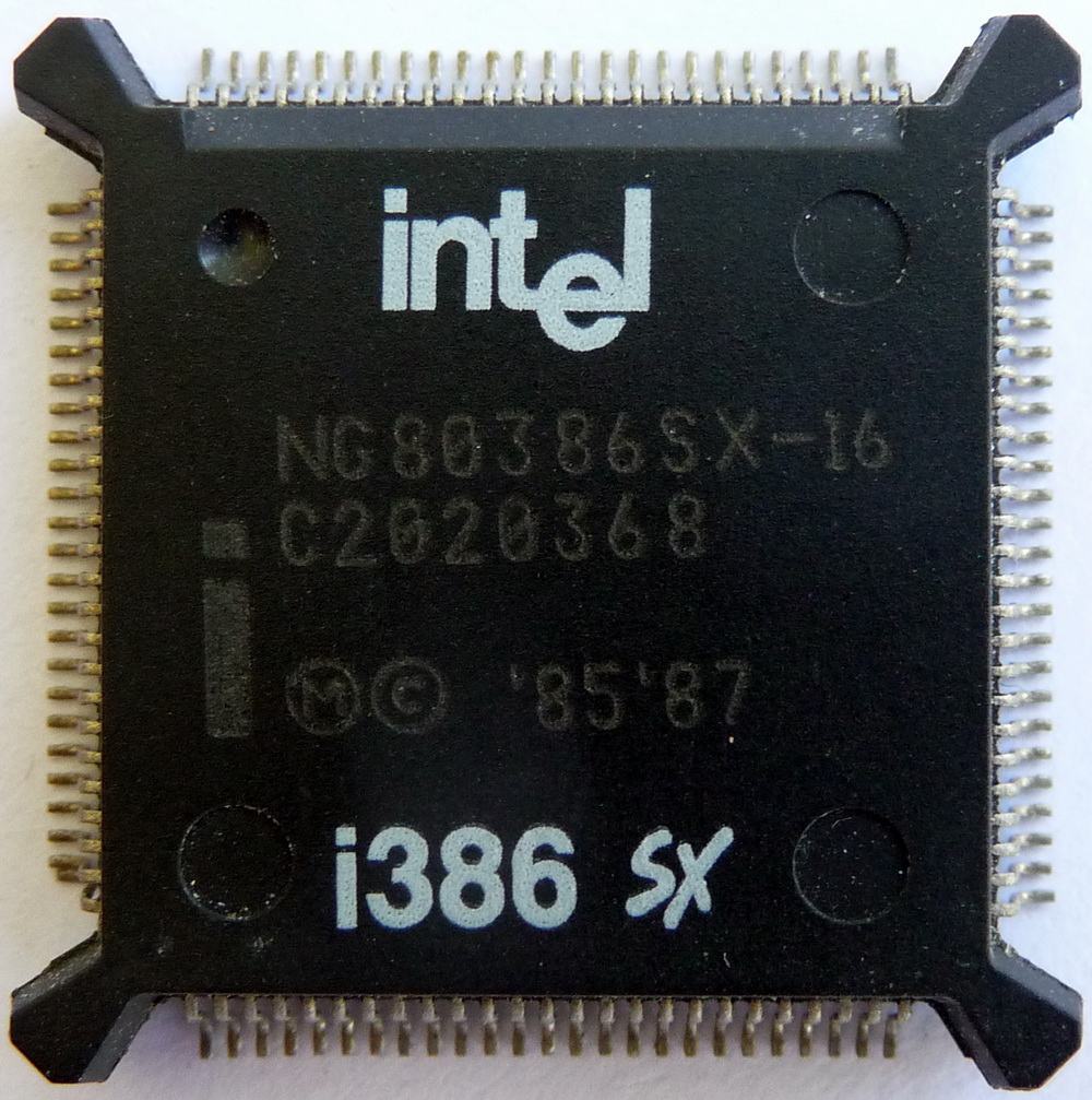 The 80386SX was a cut-down version of the 80386DX released 3 years later in 1988 around the time the 80386DX-25 was launched, with the only difference being the SX (Single-word eXternal) had a 16-bit external data bus and a 24-bit external address bus - the DX (Double-word eXternal) had 32-bit versions of both.
A low-power version of this was also produced, called the 80386SL and included power management features.
But Intel may have the advantage. For one thing, Intel has designed the 80386SX chip so it is very cheap to manufacture. Based on low-power CHMOSII technology, it is packaged in a 100-lead surface mount plastic quad flatpack. Bumpers on the corners protect the leads, thus allowing the chips to be packaged in tubes and mounted on boards by automatic handlers. And the design of the 80386SX allows it to access relatively slow and inexpensive memories effectively. As a result of its address pipelining scheme, a zero-wait-state system can be created with 100-ns DRAM.
Clock speed isn't everything. Sure, a fast 286 may run faster than a 386SX, but it doesn't mean you'll get your work done faster. Why buy a 386SX rather than a fast 286 for a few hundred dollars less? The overwhelming reason is the software you can run on a 386SX that a 286 just can't handle. Environments like DESQview 386, VM/386 and Microsoft Windows/386 and multitasking operating systems like Unix and Xenix make it possible to do true multitasking.
Intel expects to ship a 20-MHz 80386SX chip in early 1990. Because 16-MHz 386SX machines will be cheaper to produce than full-fledged 16-MHz 386 machines, the price point is likely to squeeze both the 16-MHz and 20-MHz 386 PCs out of the market. And the fast 286s will follow suit." PC Magazine, August 1989
An 80386SX will run noticeably slower than an 80386DX due to the 16-bit memory data path vs 32-bit data path. In fact, performance-wise the SX is closer to an 80286 at the same clock speed in real world terms (sometimes actually a bit slower), but does of course include the 386DX's instruction set so is able to run applications that use these such as Windows 3.x in "386 Enhanced Mode". Because of the 16-bit architecture, a 386SX can address a maximum of 16 MB of RAM (the same as the 286) compared to 4 GB with a 386DX. In reality, this 16 MB limit was more than enough for applications and games that would be able to run well on a 386SX system.
Chipset manufacturers at the time had combined chipsets that operated on both 286 and 386SX motherboards.
The 80386 was also made by licensed manufacturers including AMD (Am386DX), Chips & Technologies (K38600DX), Cyrix (Cx486DLC), MC (OEM486DLC), Texas Instruments (TI486), and IBM (386SLC).
Note that some had 486 in their chip designation - these had all the 486SX's instructions but were made to be pin-compatible with the socket on 386 motherboards, so they could run 486-compatible software. IBM's 386SLC came with an onboard 8 KB L1 cache. Cyrix' and TI's only had 1 KB.
Data sheets: 386SX Advance Information (May 1988), Cyrix 486DLC, 486SLC, 486SLCe
Programming: Programmers Reference Manual (1989)
AMD Am386
 in typical ceramic PGA package") AMD produced a rival of the 80386 called Am386. It was 100% pin- and register-compatible with the Intel 80386 (so it could run in all of its modes) but was designed to compete with the early 486s at a much more attractive price point. It was finally launched in March 1991 after numerous delays, not least being litigation with Intel over whether AMD had the right to the 386 (AMD didn't steal Intel's microcode - they actually reverse-engineered the Intel chip which was legal).
AMD produced a rival of the 80386 called Am386. It was 100% pin- and register-compatible with the Intel 80386 (so it could run in all of its modes) but was designed to compete with the early 486s at a much more attractive price point. It was finally launched in March 1991 after numerous delays, not least being litigation with Intel over whether AMD had the right to the 386 (AMD didn't steal Intel's microcode - they actually reverse-engineered the Intel chip which was legal).
It ran up to 20% faster than its Intel rival, running cooler because it used less power, and was ideal for the mobile market with it's introduction of some new features such as sleep mode and the fact it could automatically change its clock frequency from 40 MHz right down to 0 MHz depending on load. Like its Intel cousin, the Am386 did not have any internal L1 cache.
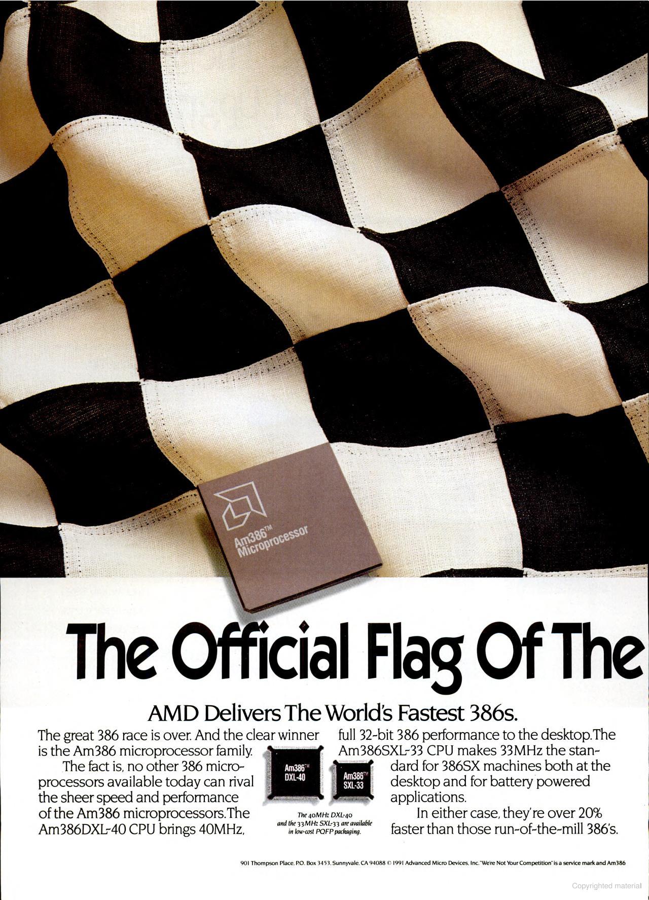
An advert for Am386 in June 1992
By the end of 1991, Am386's launch year, AMD's sales were accounting for 60% of the 386 CPU market.
 Clock speeds for the Am386 were 20 MHz, 25 MHz, 33 MHz and 40 MHz, and both SX and DX variants were available (the 20 MHz one was only available in 'DX'). Just like Intel's 80386 the DX chip had a full 32-bit external data bus interface whereas the SX chip had only a 16-bit external data bus interface.
The Am386DX was initially packaged as a PGA (Pin Grid Array), but the 40 MHz version also came in PQFP (Plastic Quad Flat Pack) which was designed to be soldered directly to the motherboard. All Am386SX CPUs came in this smaller PQFP package. In some cases the PQFP CPU was mounted on a small circuit board that allowed it to be inserted into the standard 132-pin 386 PGA socket. There is no performance difference between PGA and PQF packages.
The fastest variant, Am386-40, launched in early 1991, was also significant because it typically ran on a motherboard whose bus also ran at 40 MHz instead of the by-now-common 33 MHz. AMD claimed a 40 MHz Am386 will be faster than Intel's 486 clocked at 33 MHz in most real-world applications. These CPUs were very stable and reliable and put many 486DX-25 and -33 MHz PCs to shame for years after the consumer market had moved away from the 386 as its "go-to" processor.
Data Sheets: Am386 Data Book
Intel 80486DX
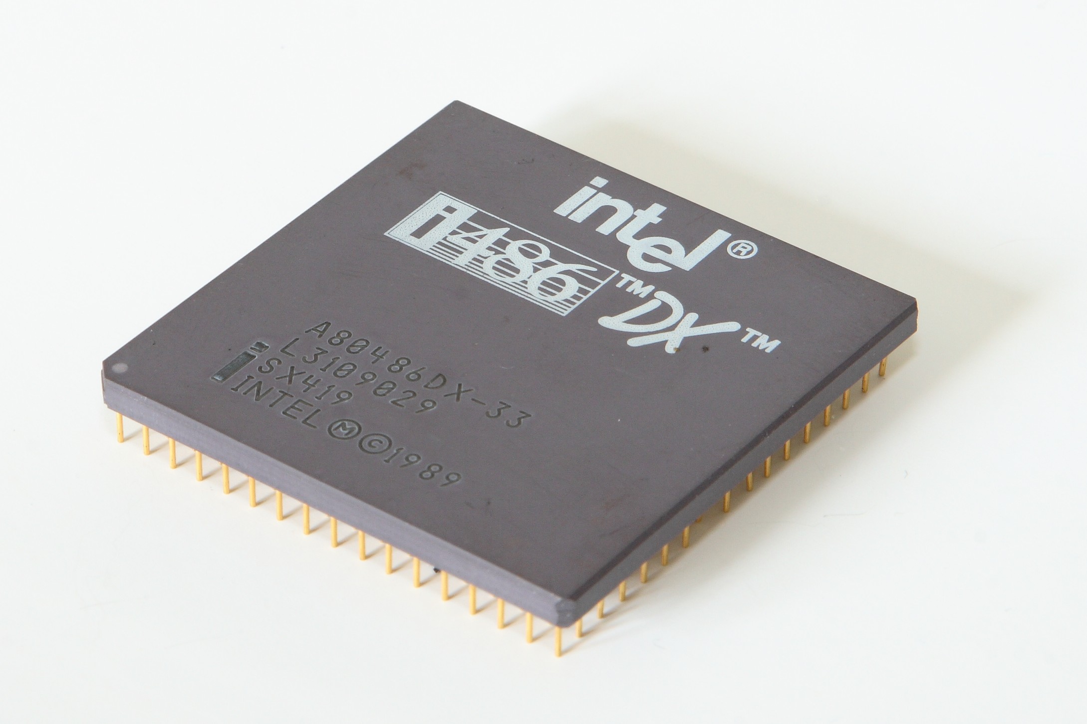 In 1989, Intel introduced its 4th generation chip, the 80486. This was a major enhancement on the 80386 microprocessor in that it added a floating point unit directly on the die (no more need for a separate math coprocessor!) as well as a fast 8 KB cache. This would become known throughout later generations of CPU as the 'Level 1' cache, and was much faster than the 80386 which only supported a slower "off-chip" cache. Furthermore, more tightly-coupled pipelining meant instructions could be processed more efficiently, improving performance. A further benefit of the 80486 was that it could now communicate with the memory subsystem at the CPU's clock speed instead of twice the clock speed which the 286 and 386 did.
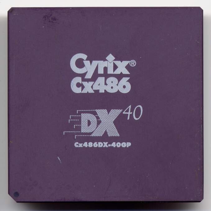
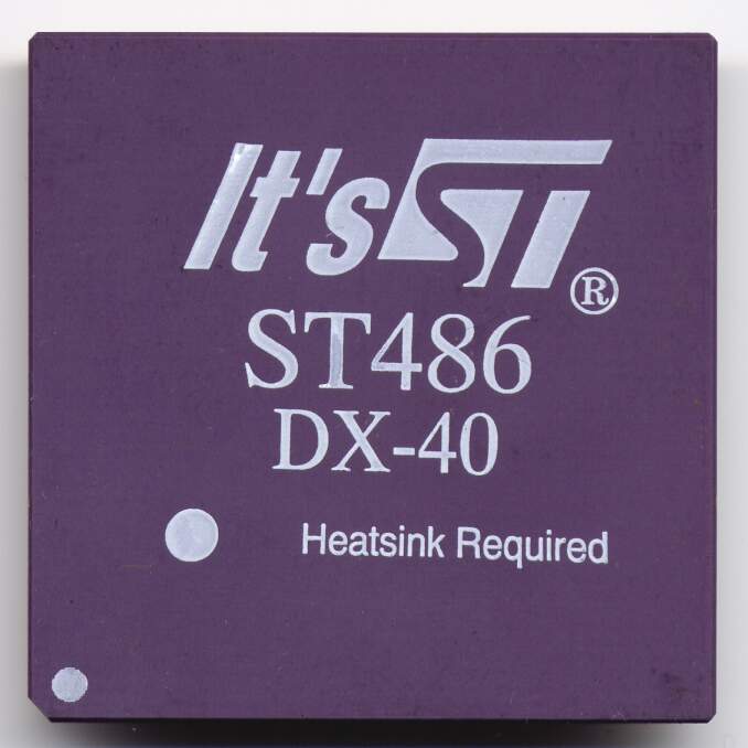
Initial versions of the 80486 came out rated at 25 MHz, but these were followed shortly with a 33 MHz version which became extremely popular. From June 1991, a 50 MHz version was made available, which was the first chip to use the new 0.8 micron circuit technology. This was also rebranded and sold by authorised chip fabricators Cyrix (named Cx486DX-50GP) and ST Microelectronics (named ST 486DX-50). By mid-1992, 486DX/50 machines were selling really well and prices were tumbling, though a shortage of the chip soon stabilised this price fall.
All 80486 CPUs were fabricated using the CMOS (Complementary Metal-Oxide Semiconductor) process, and had a 32-bit internal register size, 32-bit external data bus, and 32-bit address bus, which all matches the former 80386DX microprocessor. At any given clock rate, the "486" was roughly twice as fast as an Intel 386 (a 386DX-40 is roughly equivalent to a 486SX-20).
For backward-compatibility, the 486 is fully instruction set-compatible with previous Intel processors, but offers additional instructions, such as those to control the internal 8K cache. All of the 386s modes ("real", "protected" and "virtual real") are also fully supported. The floating-point unit (FPU) in the 486 CPU is 100% compatible with the 80387 math coprocessor, but with twice the performance.
Many 80486 motherboard designs feature a secondary cache (called the "Level 2" cache), which allows for much faster access when the 486 CPU calls for external memory. The size of this level 2 cache can vary from 16 KB up to 512 KB or more.
Intel SL Technology
Intel added a number of special features to later 486 CPUs called "SL Technology" - these were often referred to as "S" chips, or "SL Enhanced" chips. They are identifiable by an additional stamped code etched on the top of the CPU, such as &EW, &E3V1X, &E5V1X, &E5V2X and &EW5V1X. If a 486 CPU has these codes, it means the following:
| E | CPU has power-saving features including Auto Idle, enhanced HALT instruction, and Stop Clock. |
| W | Write-Back Enhanced - CPU supports write-back cache mode (faster than write-through mode). If there is no 'W' in the code your CPU only supports write-through cache mode. |
| 3V or 5V | CPU is either 3.3-volt (for mobile use) or 5-volt (for desktop use). |
| 1X or 2X | CPU is driven either by a 1x clock or a 2x clock. Earlier CPUs including 80386 required a 2x clock (the clock had to run at twice the frequency of the CPU). With the introduction of 1X, a 486 running at 25 MHz could now run with a clock that also ran at 25 MHz instead of 50 MHz. 1X allowed for simpler motherboard design by cutting in half the clock speed required in the external system, and was especially important with the introduction of the PCI bus, which would run at 33 MHz. |
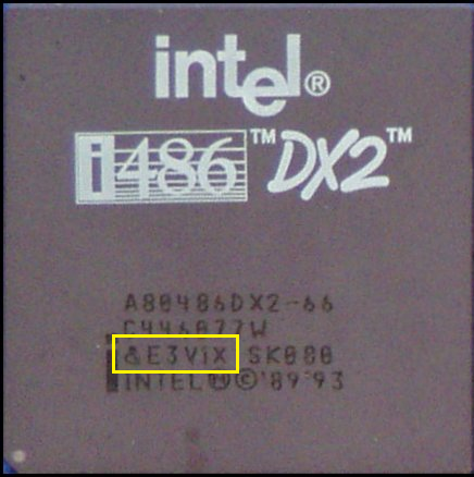
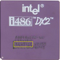
Two 486DX2-66 chips with SL Technology
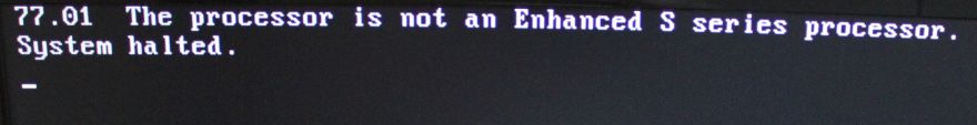
486 CPUs that have SL Technology are still fully backward-compatible with earlier non-SL CPUs, so they can still be used with motherboards that do not utilise the SL Technology features. However, some motherboards insist on an "S" CPU, and will display a warning message on POST declaring so.
Intel used the following codenames for its 486DX CPU throughout its production run:
P4 - Intel i486DX
P4S - Intel i486DX
SL Enhanced
Typical SpeedSys Score: 12.5 (80486DX-33)
Data sheets: i486 Data sheet (Apr 1989), i486 Microprocessor (Nov 1989), Intel 80486DX (Oct 1992), 486 and Related Products (Jan 1995)
Programming: Programmers Reference Manual (1990)
Intel 80486SX
 Just as with the 386, a cut-down version of the 80486 was produced called the 80486SX from mid-1991, and to now differentiate this new chip, the original 80486 was branded 80486DX. This kept the 32-bit external bus interface of the DX but omitted the integrated floating-point unit. Rumours abounded that during 1991-1992, for any 486DX chips that failed testing due to math co-processor issues, Intel simply disabled that part of it and branded it an 'SX'. This is believed to be true primarily because the die size of these early 80486SX was the same as their 80486DX brethren, while later 80486SX CPUs got a visibly smaller die size. This would prove that the 486SX started production using the 486DX mask (the photographic blueprint of the chip which is used to etch all the intricate pathways), but later got its own mask [with no FPU unit on the die].
Some 486SX motherboards provided an 'upgrade' socket next to the main CPU socket, allowing owners to later purchase either a full 486DX, a replacement 'upgrade' CPU confusingly called the i487SX (also released in 1991), or from 1992, Overdrive CPUs - if this socket was used the onboard 486SX CPU would be disabled and all instructions redirected to the new chip.
Intel used the following codenames for its 486SX CPU throughout its production run:
P23 -
Intel i486SX (with no SL Technology)
P23S - Intel i486 SL Enhanced (with SL Technology)
P23N - Intel i487SX (486 CPU but with its onboard math coprocessor enabled - if motherboard has a 487 slot, the 486SX CPU would be disabled and the 487 would take over all processing)
Clock speeds for the 80486 ranged from 16 MHz up to 100 MHz.
Typical SpeedSys Score: 9.3 (80486SX-25)
Data sheets: 486 and Related Products (Jan 1995)
Intel 80487
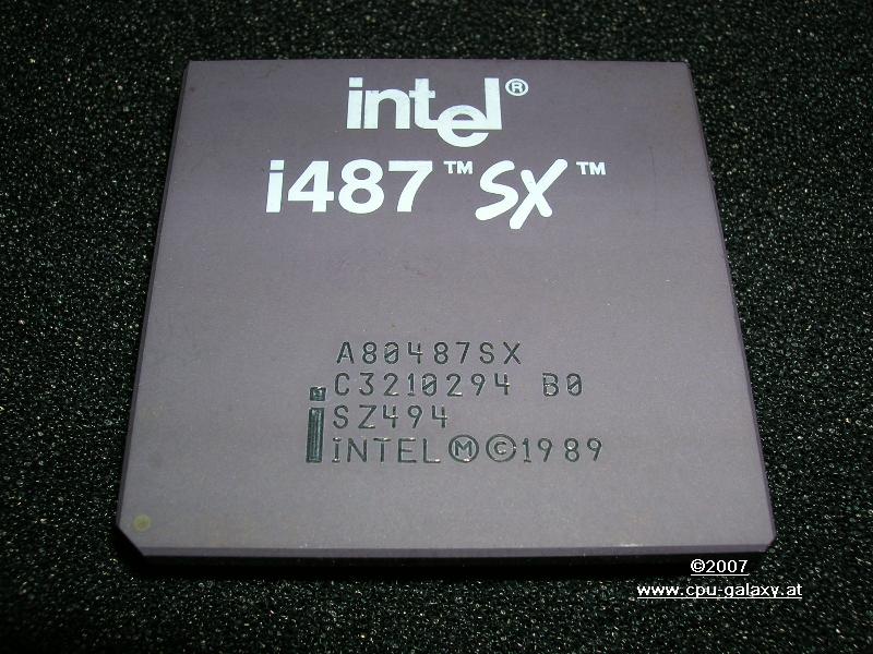 In April 1991 Intel released an upgrade chip for 386DX and 486SX owners. Called the 80487 and labelled i487SX, unlike what its name implies this was more than just a math coprocessor for 486SX owners. It was in fact a full 80486DX CPU internally, so it had an integrated FPU.
It worked both on late 386DX and 486SX motherboards, but needed the motherboard to directly support the 80487 via an "80387/80487" socket, also sometimes referred to as an "Overdrive" PGA socket. This chip had an extra pin over a standard 486DX to ensure it couldn't accidentally be put into a standard 486 CPU socket - when installed this pin tells the motherboard to disable the existing CPU, with the 80487 effectively taking over all CPU/FPU operations.
Performance was on par with dedicated 80486DX motherboards of the same clock speed - any bottleneck would be on the motherboard itself, such as the size of L2 cache.
Boards that are known to support the Intel 80487 include:
AMD Am486
 AMD were late to market with their 80486 competitor, with Intel having an almost 4-year head start. Finally, in April 1993 their Am486 was launched.
Released in 25, 33 and 40 MHz versions for the DX, and 33 and 40 MHz versions for the SX, all CPUs came with 8 KB of level 1 write-through cache (the same as Intel's), and required 5V, making them drop-in replacements for the majority of 486 motherboards. Just like its Intel counterpart, the SX had no built-in math coprocessor.
At the same time, AMD launched the Am486DXL-40. Designed to be a low-power variant of the Am486DX-40, it was otherwise identical. Later in October, they launched the 3-volt Am486DXLV which was an Am486DXL with System Management Mode (SMM) and Am486SXLV. These were only available in 33 MHz form. There was never an Am486SXL.
It's fastest non-clock-doubled chip, the Am486DX-40, provided about 20% performance gain over the Intel 80486DX-33.
CPUs in this range were:
- Am486DX-25
- Am486DX-33
- Am486DX-40
- Am486DXL-40
- Am486DXLV-33 (3V)
- Am486SX-33
- Am486SXLV-33 (3V)
- Am486SX-40
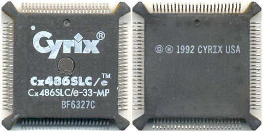
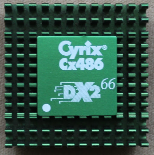
Cyrix Cx486
 in typical ceramic PGA package") Cyrix produced their own pin-compatible 80486 microprocessors with the help of various companies that could do chip fabrication (Cyrix never owned their own chip fab plant). These included IBM, Texas Instruments, and SGS Thomson. Cyrix reached an agreement with all of them that if they would manufacture their Cx486 CPUs, they could sell them too under their own brand.
Cyrix produced their own pin-compatible 80486 microprocessors with the help of various companies that could do chip fabrication (Cyrix never owned their own chip fab plant). These included IBM, Texas Instruments, and SGS Thomson. Cyrix reached an agreement with all of them that if they would manufacture their Cx486 CPUs, they could sell them too under their own brand.
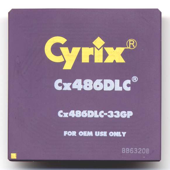
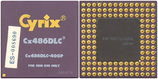
The Cx486 range started in mid-1992 with the Cx486DLC range. These were 386DX-pin compatible CPUs, but with a complete 486SX instruction set built-in and an internal 1KB cache (the same as an Intel 486SX).
Still, the Cyrix chip is attractive to a lot of vendors. It costs about the same as Intel's 25 MHz 386SL and less than half as much as Intel's 25-MHz 486SX. More important, the CX486SLC is pin-compatible with Intel's 386SX, which means PC vendors can put it into current systems by making only minor changes to the system board. Zeos will be one of the first to ship a machine with a Cyrix chip. The company is installing the chip in its 20-MHz 386SX notebook and modifying the motherboard to exploit the chip's cache. The result is a 25-MHz Cx486SLC notebook with a 100MB hard disk and 4MB of RAM that Zeos will sell for around $2,000. " PC Magazine, June 1992
Performance-wise, these came in around the same as an equivalent clock speed Intel i486SX. If you were looking to upgrade your AMD Am386DX-40 motherboard (the fastest native 386 CPU), a Cx486DLC was a great choice - much cheaper than buying the Intel i486SX. Add a matching Cyrix coprocessor, and performance was much closer to that of the i486DX and 135% that of the i386DX at the same clock.
In May 1993, Cyrix launched the Cx486S, codenamed M5 - a 486SX-compatible CPU which like Intel's did not have a built-in floating point unit (FPU). An enhancement on Intel's design though, the Cx486S came with an internal 2 KB Level 1 write-back cache as well as a "Write Burst" signal which provided some performance gains in some applications (and was motherboard-dependent).
These were labelled "FasCache". The CX486S was available only in 25, 33 and 40 MHz variants.
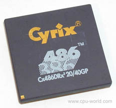
To compete with the Intel 486DX processors, in September 1993 Cyrix released the Cx486DX, codenamed M6. Like the Intel 486DX CPUs, the Cx486DX range got a massive 8 KB of Level 1 cache (4x that of the M5) and came with a built-in FPU. 25, 33, 40 and 50 MHz versions of this CPU were released. Also in 1993 they released the Cx486S2, codenamed M6n. This was a 486SX socket-compatible CPU available only in 50 MHz form and came with a 2 KB write-back cache ("FasCache"), System Management Mode (SMM), static 3.3V operation, and suspend/resume.
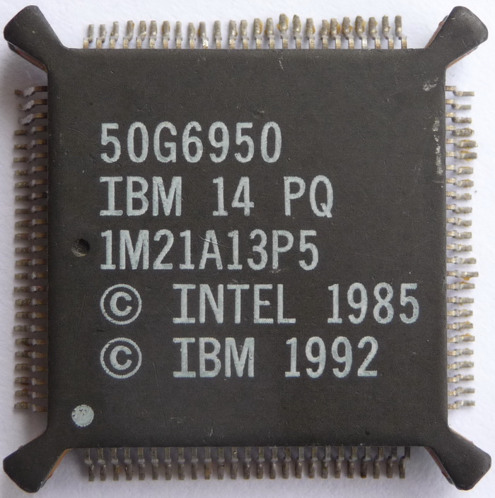
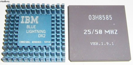
![]() IBM were authorized manufacturers and resellers of the Cyrix chips, but took their own variants up to 80 MHz, including:
IBM were authorized manufacturers and resellers of the Cyrix chips, but took their own variants up to 80 MHz, including:
- IBM 486-V50GP/QP (486DX2-50, 8 KB write-back cache, 3.3V)
- IBM 486-V66GP/QP (486DX2-66, 8 KB write-back cache, 3.3V)
- IBM 486-V150GA or QA (486DX2-50, 8 KB write-back cache, 3.3V)
- IBM 486-V266GA or QA (486DX2-66, 8 KB write-back cache, 3.3V)
- IBM 486-V466GA or QA (486DX2-66, 8 KB write-back cache, 3.6V)
- IBM 486-V666GA or QA (486DX2-66, 8 KB write-back cache, 3.45V)
- IBM 486-V380GA or GB (486DX2-80, 8 KB write-back cache, ?V)
- IBM 486-V580GA or QA (486DX2-80, 8 KB write-back cache, 4V)
The IBM chips listed above are apparently the same as the Cyrix chips internally. IBM also modified Intel's 486SL design (8 KB L1 cache, 32-bit data and address buses, internal math co-processor), with their IBM 486SLC2 and 486SLC3. These were more like enhanced 386SX CPUs, as they got a 16-bit data bus, 24-bit address bus, a whopping 16 KB of Level 1 cache, a full 486SX instruction set, no math co-processor, but were clock-multiplied (SLC2=clock-doubled, SLC3=clock-tripled). IBM never created a non-clock-multiplied 486SLC.
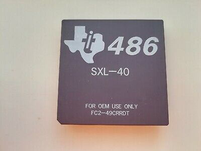
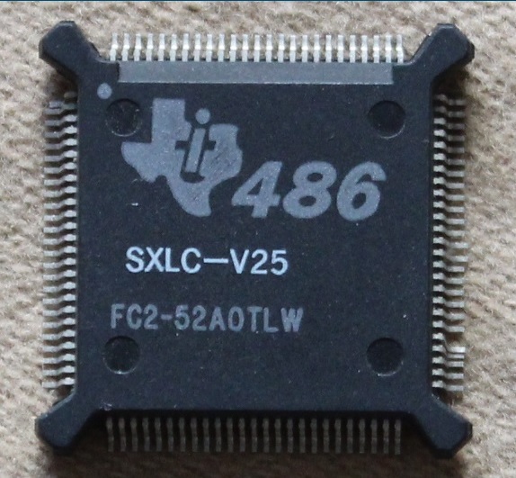
![]() The Texas Instruments SXL range were unique from the Cyrix and IBM range in that TI created their own micro-architecture on top of the Cyrix design, and this range was codenamed 'Potomac'. Produced in both non-clock doubled and clock doubled/tripled form, and also in 132-pin form for 386DX motherboards and 168-pin form for 486 motherboards, there is quite the selection! The SXL range are backward-compatible with the TI486DLC/E range. In fact, the only difference between the 486SLC/DLC family and the 486SXL[C] family is the cache size (8 KB on SXL instead of 1 KB on SLC/DLC), cache organisation (SXL has 2-way set associative cache, SLC/DLC has 2-way or direct-mapped cache - both were write-through), and the clock-doubling feature (the 486SXL family support clock doubling, the SLC/DLC range do not).
The Texas Instruments SXL range were unique from the Cyrix and IBM range in that TI created their own micro-architecture on top of the Cyrix design, and this range was codenamed 'Potomac'. Produced in both non-clock doubled and clock doubled/tripled form, and also in 132-pin form for 386DX motherboards and 168-pin form for 486 motherboards, there is quite the selection! The SXL range are backward-compatible with the TI486DLC/E range. In fact, the only difference between the 486SLC/DLC family and the 486SXL[C] family is the cache size (8 KB on SXL instead of 1 KB on SLC/DLC), cache organisation (SXL has 2-way set associative cache, SLC/DLC has 2-way or direct-mapped cache - both were write-through), and the clock-doubling feature (the 486SXL family support clock doubling, the SLC/DLC range do not).
![]() Note though that the 168-pin chips do need a 486 motherboard (and BIOS) that directly supports it if the larger cache size and clock-doubling features are to be used. Performance-wise the TI SXL microarchitecture is about 30% slower than an Intel 486DX running at the same clock speed on an integer benchmark. Also interesting is that the 'B0' stepping of the SXL and SXL2 are identical - this means a straight SXL can also be made to run in clock-doubled mode! Stepping 'A0' probably does not support this feature as it is lacking SMI support and likely does not have the internal PLL (phase-locked loop) circuitry.
Note though that the 168-pin chips do need a 486 motherboard (and BIOS) that directly supports it if the larger cache size and clock-doubling features are to be used. Performance-wise the TI SXL microarchitecture is about 30% slower than an Intel 486DX running at the same clock speed on an integer benchmark. Also interesting is that the 'B0' stepping of the SXL and SXL2 are identical - this means a straight SXL can also be made to run in clock-doubled mode! Stepping 'A0' probably does not support this feature as it is lacking SMI support and likely does not have the internal PLL (phase-locked loop) circuitry.
The 168-pin "486-motherboard-compatible" range were:
- Cyrix Cx486S-25 FasCache (2 KB write-back cache, no FPU, 5V). Released in May 1993. No heatsink.
- Cyrix Cx486S-33 FasCache (2 KB write-back cache, no FPU, 5V). Released in May 1993. Permanent heatsink.
- Cyrix Cx486S-40 FasCache (2 KB write-back cache, no FPU, 5V). Released in May 1993. Permanent heatsink.
- Cyrix Cx486DX-33 (8 KB cache, FPU, 5V). Released in Sep 1993. No heatsink.
- Cyrix Cx486DX-40 (8 KB cache, FPU, 5V). Released in Sep 1993. Permanent heatsink.
- Cyrix Cx486DX-50 (8 KB cache, FPU, 5V). Released in Sep 1993. Permanent heatsink.
- ST Microelectronics ST486DX-40 (8 KB cache, FPU, 5V). Released in Sep 1994.
- All the IBM Blue Lightning 486-V chips mentioned above
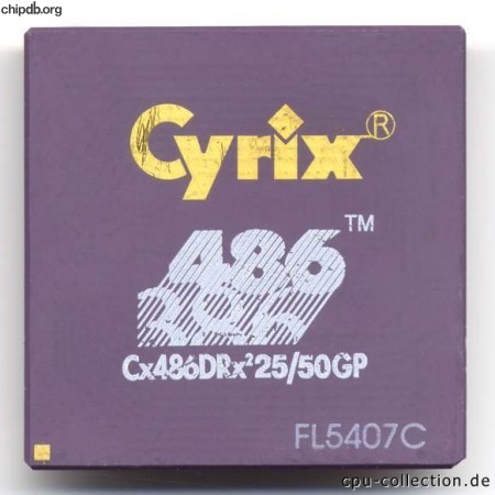
The Cx486DRx2 33/66 allows users of 33-MHz 386 systems to upgrade to 486-level performance, offering about twice the performance of a 33-MHz 386 processor, Cyrix said. The chip is easy to install in more than 15 minutes, according to the company. The complete upgrade kit comes with the upgrade processor, tools to remove the old 386 processor, and cache-installation software.
The cache software is installed under DOS, Windows, or OS/2. The chip is available now and is priced at $399. The Cyrix upgrade communicates with the system at 33 MHz, the same speed of the 386, while it runs at 66 MHz internally, identical to Intel Corp.'s fastest 486 DX2 chips. But the upgrade only offers a 1KB on-chip cache compared to Intel's 8KB. Cache size, in many applications, can have a major impact on performance. Larger caches usually offer better performance.
Intel's DX and DX2 486 processors also have on-chip floating-point units, and Cyrix's upgrades do not.
The 486DRx2 33/66 uses the same microprocessor core as the company's 20/40 and 25/50 chips - upgrades already on the market for 386 20-MHz processors and 386 25-MHz processors. " Info World, 4th April 1994
The 132-pin "386DX-motherboard-compatible" range were (note: always check it has 132 pins not 168, as these were sold in both forms!):
- Cyrix Cx486DLC-33GP (1 KB L1 cache, no FPU, 5V). Released in Jun 1992.
- Cyrix Cx486DLC-40GP (1 KB L1 cache, no FPU, 5V). Released in Jun 1992.
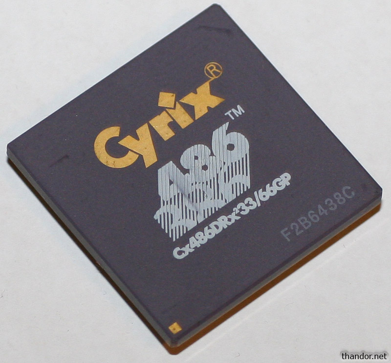
- Cyrix Cx486DRx2/40GP (1 KB L1 cache, no FPU, 5V). Released in Sep 1993.
- Cyrix Cx486DRx2/50GP (1 KB L1 cache, no FPU, 5V). Released in Sep 1993.
- Cyrix Cx486DRx2/66GP (1 KB L1 cache, no FPU, 5V). Released in Sep 1993.
- IBM 486SLC2-50 (16 KB cache, no FPU, 5V). Released in Dec 1992.
- IBM DLC3 (16 KB cache, no FPU, 5V)
- Texas Instruments TI486SXL-40 (8 KB L1 WT cache, no FPU, 5V).
- Texas Instruments TI486SXL-G40 (8 KB L1 cache, no FPU, 3.3V). 5V-tolerant I/O*.
- Texas Instruments TI486SXL-V40 (8 KB L1 cache, no FPU, 3.3V). 3.3V only.
- Texas Instruments TI486SXL2-G40 (8 KB L1 cache, no FPU, 3.3V). 5V-tolerant I/O*.
- Texas Instruments TI486SXL2-50 (8 KB L1 cache, no FPU, 5V).
- Texas Instruments TI486SXL2-G50 (8 KB L1 cache, no FPU, 3.3V). 5V-tolerant I/O*.
- Texas Instruments TI486SXL2-V50 (8 KB L1 cache, no FPU, 3.3V). 3.3V only.
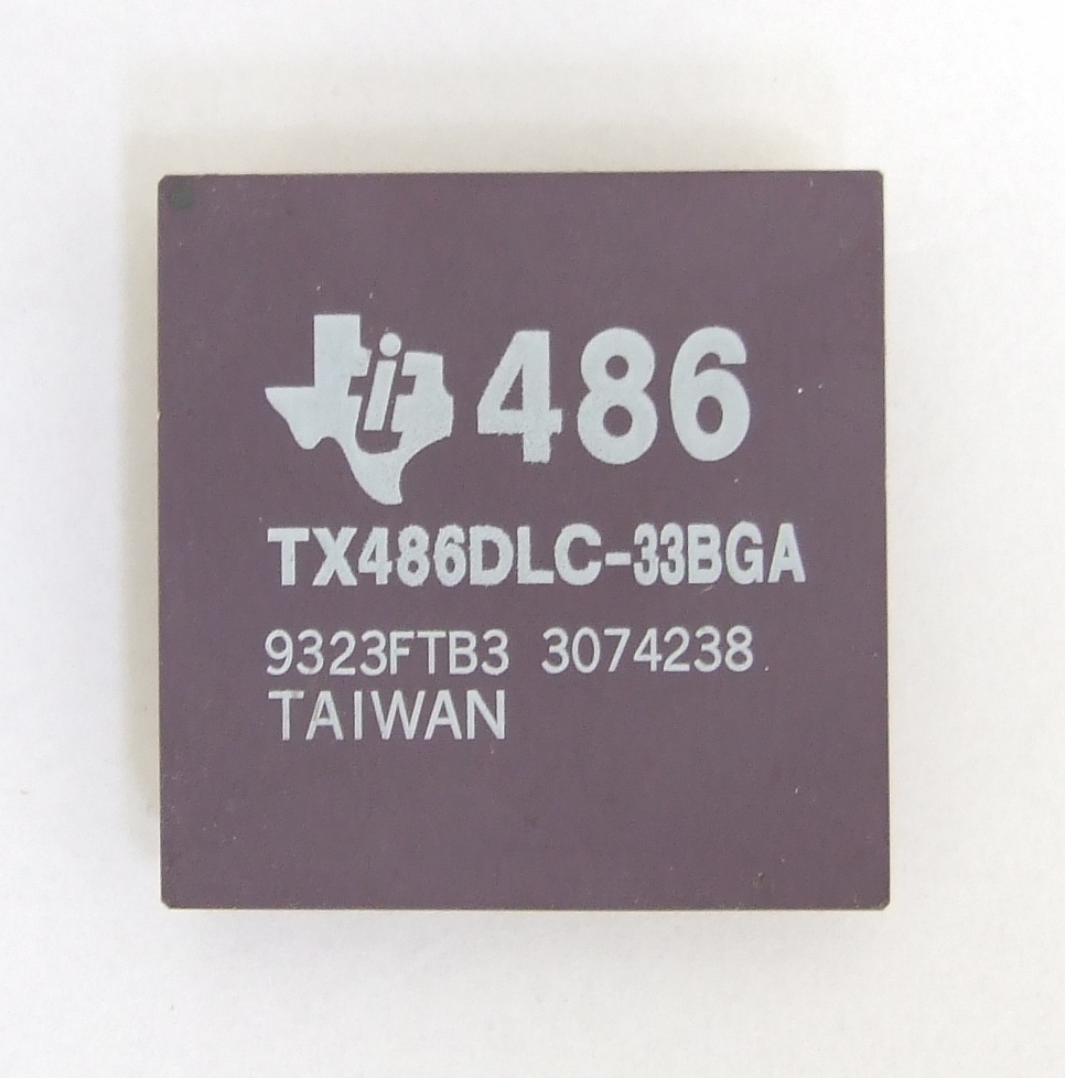
- Texas Instruments TX486DLC-33 or TI486DLC/E33 (1 KB L1 cache, no FPU, 5V). Released in Jun 1992.
- Texas Instruments TX486DLC-40 or TI486DLC/E40 (1 KB L1 cache, no FPU, 5V). Released in Jun 1992.
*Important: Do not mis-read this! 5V-tolerant I/O does *not* mean the CPU will work in a 5V CPU socket. These CPUs still require a 3.3V core voltage and will be damaged if given a 5V core. It just means these CPUs can work in boards that have either only 3.3V or mixed 3.3V and 5V I/O voltage supply to the CPU.
The DRx2 chips from TI are 386DX-compatible but also contain a 486 instruction set. As the name suggests these are clock-doubled versions of the DRx chips. They do *not* come with a built-in FPU. They make better drop in upgrades for older systems since they have a built in cache coherency circuit. The stock Cyrix and TI DLC/SLC/SXL chips normally require an adapter or a modification to work properly with the cache enabled.
The 132-pin "386SX-motherboard-compatible" range are listed below. The 'C' in the TI part numbers denotes 16-bit I/O, whereas no 'C' in the part number means 32-bit I/O, hence why the 'C' ones are designed for 386SX motherboards only, and the non-'C' ones are designed only for 386DX motherboards. These are in a 100-pin QFP (Quad Flat Pack) package, and are fully backward-compatible with the TI486SLC/E range):
- Cyrix Cx486SLC-25 (1 KB L1 cache, no FPU, 5V). Released in Dec 1992.
- Cyrix Cx486SLC-33 (1 KB L1 cache, no FPU, 5V). Released in Dec 1992.
- Texas Instruments TI486SXLC-V25 (8 KB L1 cache, no FPU, 3.3V).
- Texas Instruments TI486SXLC-040 (8 KB L1 cache, no FPU, 5V).
- Texas Instruments TI486SXLC2-050 (8 KB L1 cache, no FPU, 5V). Basically a Cyrix SXL2.
All these chips were successful for consumers looking to upgrade, due to their lower price point over Intel, although performance clock-for-clock against Intel's and AMD's equivalent CPUs was generally poorer.
Note: DLC chips do run very hot, so these days it is highly recommended you use a heatsink even though historically it was never a requirement.
Intel 80486DX2 / 80486DX4
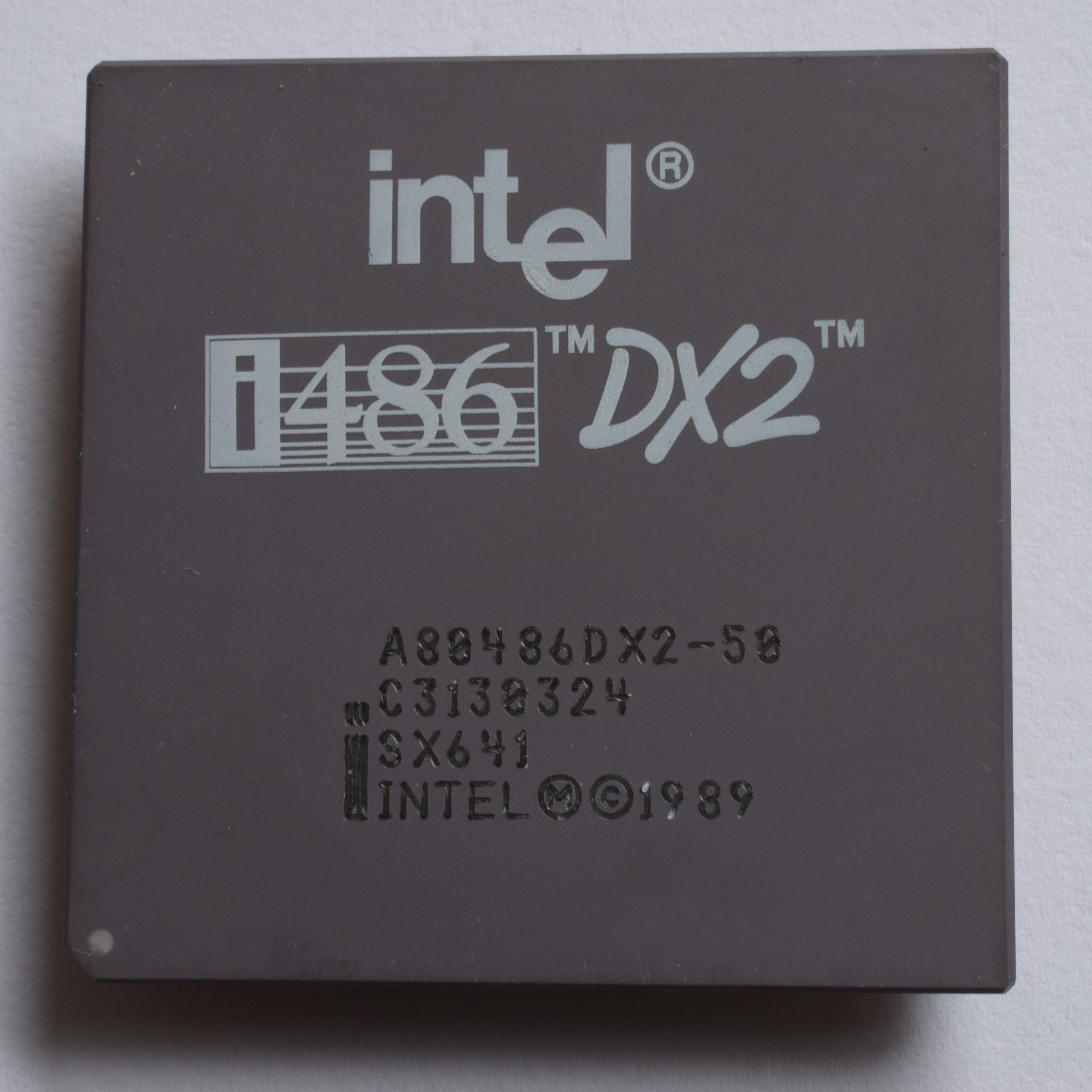 In 1992, alongside the Overdrive processors (see further down) Intel released the new 80486DX2. This doubled the internal CPU clock without any changes being necessary external to the CPU, resulting in largely a 100% performance increase. This was made possible partly thanks to the 486's internal (Level 1) 8 KB cache which helped mask slow memory access. The 80486DX2 CPUs still ran at the same 5V as the original 486 CPUs.
Intel released the 80486DX2 CPU in 50 MHz (clock-doubled 486DX-25) and 66 MHz (clock-doubled 486DX-33) variants. Both were available in the P24[S] and later P24D version, where P24[S] only had the write-through cache, and P24D came with the faster L1 cache (called "write-back"). P24D had the marking "&EW". P24S had "&E" (no 'W') on it.
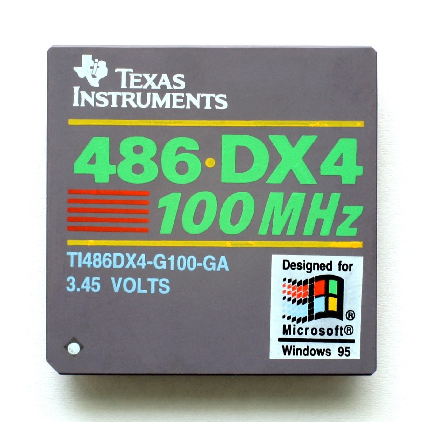
In late 1994, the first clock-tripled processors were released, confusingly called 80486DX4, rather than 80486DX3. These reduced the core voltage from 5V down to 3.45V in order to run cooler, which meant they could not be installed in older 5V-only sockets. You needed to have a motherboard that could have the core voltage adjusted down to 3.3V in order to support a 486DX4. In some cases, vendors offered a 3.3v voltage adapter to install the chip into a 5V socket. These adapters had jumpers that allowed you to select the DX4 clock multiplier (2x, 2.5x, or 3x mode). One key difference between the earlier DX2 and the later DX4 is that DX2 always operated internally at double the motherboard clock speed (the external "bus frequency"), whereas DX4 processors operate at 2, 2.5, or 3x the motherboard clock rate. Apart from the clock frequency and voltage differences, DX4 is the same as DX2.
Intel released the 80486DX4 CPU in 75 MHz (clock-tripled 486DX-25) and 100 MHz (clock-tripled 486DX-33) variants.
It is prudent to note that around this time VESA Local Bus was prevalant. This bus, which was designed to enable faster graphics cards, was notorious for not playing well with higher bus speeds.
Intel used the following codenames for its 486DX2 and 486DX4 CPUs throughout its production run:
P24 -
Intel i486DX2 (8KB WT (write-through) L1 cache, 5V)
P24S - Intel i486DX2 SL Enhanced (8KB WT L1 cache, 5V)
P24D - Intel i486DX2 Write Back Enhanced (8KB WB (write-back) L1 cache, 5V)
P??? - Intel i486SX2 (8KB WT L1 cache, 5V)
P24C - Intel i486DX4 (16KB WT L1 cache, 3.3V)
P??? - Intel i486DX4 Write Back Enhanced (16KB WB L1 cache, 3.3V)
Data sheets: 486DX2 data sheet (Feb 1992), 486 and Related Products (Jan 1995)
AMD Am486DX2 / Am486DX4
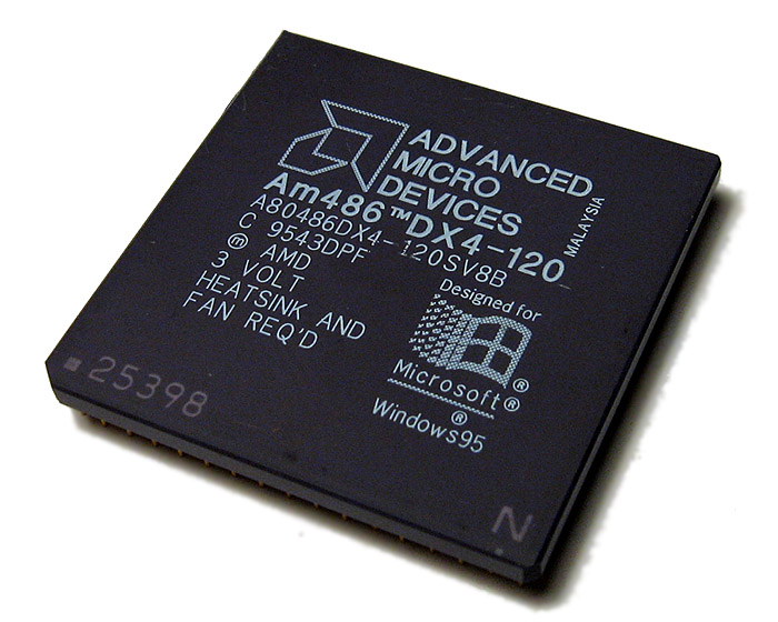 AMD produced a clone of both the Intel 80486DX2 from April 1993, and 80486DX4 CPUs from September 1994.
The AMD Am486DX2 was released in 50 MHz and 66 MHz variants, just like Intel's, but they then took it one step further with an 80 MHz variant (a clock-doubled DX-40).
Moving to the clock-tripled chips, the Am486DX4 was released in 75 MHz and 100 MHz variants (the same as Intel), but again took it one step further with a 120 MHz version (you guessed it, a clock-tripled DX-40), making this the fastest CPU available at the time for the Socket 3 platform. Just as with the Intel chips, clock tripling means that the CPU contains multiplier circuitry built-in so operations within the CPU run at three times the frequency, whilst operations outside the CPU (the bus to the memory) run at one times the frequency. So an AMD Am486DX4-100 runs at 100 MHz within the CPU, but 33 MHz when accessing RAM.
All have an 8 KB Level 1 cache apart from the Am486DX2-66V16BGC, which came with an incredible 16 KB write-back L1 cache.
The Am486DX2-50 still required 5V core voltage, but the 66 and 80 MHz versions required 3.3V core voltage.
All Am486DX4 CPUs require 3.3V core voltage to power them, making them unsuitable for older Socket 3 motherboards that only support 5V CPUs. Be sure to check your motherboard supports 3.3V and set the CPU voltage jumpers correctly before powering on!
The AMD 486DX4-100 dissipates 2.6W of heat, whilst the 486DX4-120 dissipates 3.2W.
Some AMD 486DX4-100 CPUs apparently support only 2x and 3x multipliers while others support 3x and 4x multipliers. If you have 16 KB of L1 cache then your CPU is the same as an AMD 5x86-P75. If you have only 8 KB of L1 cache then it's not the same, even if it has WB ("write-back") cache.
Following on from their low-power, non-clock-doubled range (Am486DXL and Am486SXL), AMD produced Am486DXL2 which came in 66 and 80 MHz versions. There was never an Am486SXL2 but they did release Am486SX2 in 50 and 66 MHz versions.
In all, here is the list of AMD Am486DX2 and DX4 chips (WT = Write-Through cache, WB = Write-Back cache):
- Am486DX2-50
- Am486SX2-50
- Am486DX2-66
- Am486SX2-66
- Am486DX2-66 Enhanced WT (NV8T or V8TGC), Enhanced WB (SV8B or V16BGC)
- Am486DXL2-66
- Am486DX2-80 Enhanced WT (V8T or NV8T)
- Am486DXL2-80
- Am486DX4-75
- Am486DX4-90 Enhanced WT (NV8T)
- Am486DX4-100
- Am486DX4-100 Enhanced WT (NV8T), Enhanced WB (SV8B or V16BGC or SV16BGI)
- Am486DX4-120 Enhanced WT (NV8T), Enhanced WB (SV8B)
Typical SpeedSys score:
Am486DX4-100 = 37.5
Am486DX4-120 = 44.5
Cyrix / IBM / SGS Thomson 486DX2/DX4
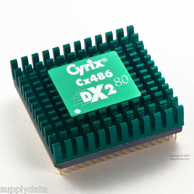
 In September 1993, Cyrix launched their first clock-doubled 486s (codenamed M7), the Cx486DX2-50 and Cx486DX2-66. These were based on the M6 design (Cx486S2/50) but got a larger FasCache and higher clock speeds.
A low-voltage variant was also released, called the Cx486DX2-V66. Later, a Cx486DX2-80 was also made available, which was a clock-doubled version of its Cx486DX-40. These were the first ones to come with a nice dark green anodised heatsink on top. IBM did the same a little later for their variants, except theirs were coloured electric blue instead of green. IBM ones were only available with the purchase of an IBM PS/2 or server.
Texas Instruments produced their licenced versions too. Unlike other approved fabricators TI insisted on adding a way to distinguish their CPU from other brands. This was implemented by setting a bit (DIR1[7]) in one of the Cyrix-specific registers. If the bit is “1”, the CPU is TI-branded. If the bit is clear, it’s a Cyrix, IBM or ST 486. Bear in mind the voltages on these TI chips were all 3.45V, not 5V, so do check your motherboard to ensure compatibility.
L1 cache sizes on these were the same as Intel's at 8 KB in size.
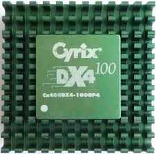
A single clock-tripled version was launched exactly 2 years later- the Cx486DX4-100.
The variants of these chips were:
- Cyrix Cx486DX2-50 and -66 (8 KB L1 cache, FPU, 5V). Released in Sep 1993.
- Cyrix Cx486DX2-V66 (8 KB L1 cache, FPU, 3.3V or 3.45V). Released in Sep 1993.
- Cyrix Cx486DX2-80 (8 KB L1 cache, FPU, 5V). Released in Nov 1994.
- Cyrix Cx486DX2-V80 (8 KB L1 cache, FPU, 3.45V or 4V).
- Cyrix Cx486DX4-100 (8 KB L1 cache, FPU, 3.45V). Released in Sep 1995.
- IBM 486DX2-50 (8 KB L1 cache, FPU, 5V)
- IBM 486DX2-66 486-V266GA or 486-V666GA (8 KB L1 WT cache, FPU, 5V)
- IBM 486DX2-80 (8 KB L1 cache, FPU, 5V). Released in Feb 1995.
- IBM 486DX4-100 (8 KB L1 cache, FPU)
- Texas Instruments TI486DX2-66 TI486DX2-G66-GA (8 KB L1 WT cache, FPU, 3.45V, PGA)
- Texas Instruments TI486DX2-66 TI486DX2-G66-WR (8 KB L1 WT cache, FPU, 3.45V, QFP)
- Texas Instruments TI486DX2-80 TI486DX2-G80-GA (8 KB L1 WT cache, FPU, 3.45V, PGA)
- Texas Instruments TI486DX4-100 TI486DX4-G100-GA (8 KB L1 WT cache, FPU, 3.45V, PGA)
- Texas Instruments TI486DX4-100 TI486DX4-G100-WR (8KB L1 WT cache, FPU,3.45V, QFP)
- Texas Instruments TI486DX4-100 TI486DX4-GT100-GA (8 KB L1 WB cache, FPU, 3.45V, PGA)
- Texas Instruments TI486DX4-100 TI486DX4-GT100-WR (8KB L1 WB cache,FPU,3.45V, QFP)
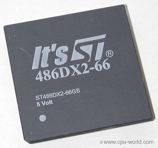
- ST Microelectronics ST486DX2-50 (8 KB L1 cache, FPU, 5V)
- ST Microelectronics ST486DX2-66 (8 KB L1 WT cache, FPU, 5V). Released in Sep 1994.
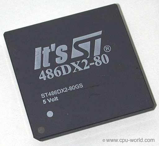
- ST Microelectronics ST486DX2-80 (8 KB L1 cache, FPU, 5V). Released in Sep 1994.
- ST Microelectronics ST486DX4-100 (8 KB L1 cache, FPU, 3.45V)
Intel 80486 Overdrive
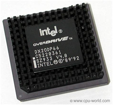 i486 Overdrive processors (not to be confused with the later Pentium Overdrive) can be considered an 'extension' of the 80486 family, primarily used to extend the functional life of a PC with an older 486 motherboard through increased performance. These overdrive processors were actually 3.3V CPUs, but came with built-in voltage regulators which allowed an input voltage of 5V from the motherboard. These CPUs got write-back cache in place of the write-through cache, and came with a fixed heatsink on top.
Launched in 1992 alongside the new 80486DX2 CPUs, Overdrive CPUs came in two distinct versions - those that were designed to fit into a special 'overdrive' socket on the mainboard (these CPUs had an 'ODP' designation, for 'OverDrive Processor'), and those that were designed to replace the existing CPU entirely (with 'ODPR' designation - I guess the 'R' stands for 'Replacement').
The plan was that for existing 80486SX users (with no floating point unit), the ODP would give them an FPU as well as clock-doubling, whereas for 80486DX users who already had the integrated floating-point unit (FPU) in their CPU, the ODPR Overdrive would still be an attractive option as they could still get the massive performance advantage of clock-doubling. When using these clock-doubled chips, it was more important than ever to have a good-sized Level 2 cache on the motherboard to realise the greatest performance gain. The Level 2 cache greatly reduces the number of wait states that the processor will have to add when writing to system memory or when a read causes an internal cache 'miss'. Motherboards that have no external (level 2) cache will still enjoy a near-doubling of CPU performance but operations that involve a great deal of memory access will be slower.
Overdrive chips required the built-in heatsink because doubling the internal clock increased the heat output dramatically (remember these still take in 5V from the motherboard, just as all CPUs from the 1st generation up to this 4th generation were).
The ODP chips had an additional pin (169 pins in total) to ensure they could not be mistakenly inserted into an existing 168-pin CPU socket.
The designation was easily identifiable on the chip's model number, e.g. "DX2ODPR66". Until around 1994, the chip designations for Overdrive chips reflected the CPU it was meant to replace, e.g. ODPR486SX-33 was meant to replace a 486SX-33, but it actually ran at a clock-doubled 66 MHz. Sometime in 1994, Intel changed this designation to reflect the actual new speed, e.g. DX2ODPR66.
Later, with the launch of the 80486DX4, Intel launched clock-tripled Overdrive processors too as an upgrade path for customers with older 486 CPUs. Just as with the clock-double ones, all clock-tripled (DX4) Overdrive processors got a built-in voltage regulator, as their core now ran at 3.45V instead of 5V. The voltage regulator allowed these processors to still be used in older 5V-only 486 sockets.
The following Intel Overdrive chips were available:-
Clock-doubled:
DX2ODP[R]40 - 40 MHz core, 20 MHz front-side bus - $549 (initial retail price)
DX2ODP[R]50 - 50 MHz core, 25 MHz front-side bus - $699 (initial retail price)
DX2ODP[R]66 - 66 MHz core, 33 MHz front-side bus
Clock-tripled:
DX4ODP[R]75 - 75 MHz core, 25 MHz front-side bus
DX4ODP[R]100 - 100 MHz core, 33 MHz front-side bus
So basically, the Overdrive CPUs really were just retail versions of the clock-doubled DX2 or clock-tripled DX4 with voltage regulators that allowed them to work on older 5V motherboards. DX4 Overdrives were still being marketed by Intel at least until 1997, when their prices had dropped to just $159 for the 75 MHz variant, and $209 for the 100 MHz variant.
Intel used the following codenames for its 486 Overdrive CPUs throughout its production run:
P4T - Intel i486 Overdrive (clock-doubled)
P23T - Intel i486 Overdrive (clock-tripled)
Typical SpeedSys Score: 25 (80486DX2-66), 40 (80486DX4-100)
Data sheets: 486 and Related Products (Jan 1995)
AMD 5x86
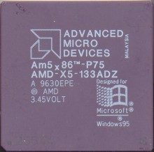 AMD began to branch away from Intel's designs with the introduction of their "5x86" CPU in November 1995, codenamed "X5" or "Am486Plus". This was supposed to be a stop gap between their aging Am486 chips and the yet-to-be-released K5 series. Despite this designation of "5x86" that implied a 5th-generation architecture, i.e. Pentium, the 5x86 was essentially a fast Intel 80486DX4 (or more specifically, AMD 486DX4), but with a built-in preset clock multiplier of 4x instead of the DX4's 3x multiplier. This allowed it to run at 133 MHz on motherboards that have no native support for Intel clock-doubled or clock-tripled CPUs. This made it a favourable upgrade option for those who had an aging Socket 3 motherboard, but wanted a lot more power.
The AMD 5x86 featured a 16 KB level 1 write-back cache, which was considered generous at the time. It was released in only two clock speeds - 133 MHz and 150 MHz - and ran at this speed on 33 MHz FSB Socket 3 motherboards (four times the bus speed).
In order for the 5x86 to work with the older Socket 3 design which was never designed to support a 4x clock multiplier, the CPU would look for a motherboard [or BIOS] setting of 2x multiplier (as this was the highest a Socket 3 board could multiply the clock), and would internally run the CPU at 4x instead. This means when you're configuring your Socket 3 motherboard's jumpers you need to choose the '2x' setting for the CPU multiplier.
Bear in mind also that the AMD 5x86 is a 3.3V chip, not 5V, so be sure to confirm your motherboard natively accepts 3.3V core voltage CPUs. This is especially important on Socket 1 and 2 motherboards. Some Socket 3 boards have a CPU voltage jumper to allow you to set it to either 3.3V or 5V. If you don't see this, your motherboard is almost certain to only accept 5V CPUs so you *must* use a CPU voltage regulator.
With the benefit of the 4x clock multiplier and "huge" L1 cache, the 133 MHz 5x86 was a little faster than an Intel 80486DX4-100, and even beat Intel's Pentium 75 in synthetic benchmarks. This is why it has "-P75" stamped on the chip, to give an indication as to its performance when compared to an Intel CPU.
In order to get the most benefit from the 5x86, it's a good idea to have a large Level 2 cache on the motherboard. This helps prevent bottlenecks when accessing memory with such a fast CPU running on a much slower board.
Typical SpeedSys Scores: 45 (AMD 5x86C-100), 54.5 (AMD 5x86-P75, aka X5-133)
Cyrix 5x86
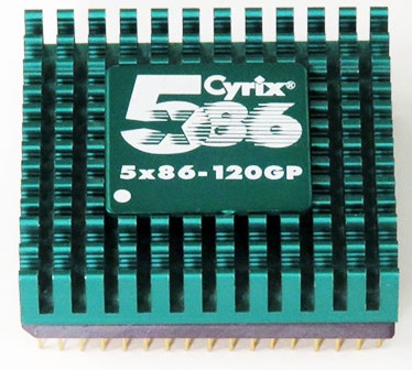 Unlike AMD who pressed on with the fourth generation, Cyrix jumped on the new fifth-generation Pentium bandwagon in June 1995 with their rival CPU called the 5x86. This was a 'lite' version of their upcoming 6x86 (M1) core, so it had the codename "M1sc". It featured Pentium-like 64-bit internal addressing, 6-stage "super-pipelining" and branch prediction technologies, and came with a 16 KB level 1 cache.
Designed to be used on existing 486 motherboards, the Cyrix 5x86 was packaged the same as an Intel 486 (same 168-pin configuration in a PGA (pin grid array) package), but the motherboard needed to have specific support in its BIOS for this chip. Usually it was installed into a P24D (80486DX2 with write-back cache) socket on a late Socket 3 motherboard. It can run on earlier 486 motherboards if a voltage regulator is used, since the 5x86 is a 3 volt chip and earlier 486 boards were all 5 volts.
The CPU actually runs in a clock-tripled way, just like the Intel 486DX4 chips, so it runs on 33 MHz and 40 MHz motherboards - the 100 MHz version can also run on 50 MHz x 2 (clock-doubled) but is more commonly run at 33 MHz x 3.
The 5x86 incorporated excellent power-saving technology where it would shut down parts of its internal circuitry unless it was called upon.
Clock speeds ranged from 80 MHz up to 133 MHz, although the latter are very rare having only been made in small quantities for a different manufacturer, Evergreen. The most common are the 100 MHz and 120 MHz versions. The 120 MHz version of the Cyrix 5x86 is about 25% faster than the AMD 5x86-P75 (very much a 486 design) and about 30% faster than an Intel 486DX4-120, making it the fastest CPU that will run on a 486 board alongside the AMD X5-133 or X5-160, with comparable performance to a Pentium 90 or 100. Cyrix also licensed IBM and SGS-Thomson to use the 5x86 design (these two actually manufactured Cyrix' own chips for them in their fabrication plants, since Cyrix did not have their own).
The following motherboards are known to support the Cyrix 5x86 range:
- ABIT PM4T v10 (with Award BIOS revision 4.5)
- ASUS PVI-486SP3 v1.21 (with Award BIOS revision 0301)
- Biostar MB8433-UUD
- Biostar MB1433UIV v7 (with AMI BIOS dated 7/24/95)
- DFI G486VPA Revision A
- ECS UM8810P AIO v2 (with Phoenix BIOS rev 4.04)
- EFA 486U-PIO
- FIC 486PIO2
- FIC 486PVT
- FIC 486PVT-IO
- PC Chips M919
- PC Chips M921
Typical SpeedSys Score: 73.41 (Cyrix 5x86-133 greatly overclocked)
Data sheet: Cyrix 5x86 (Jul 1995)
Cyrix 5x86 Processor Brief
Intel Pentium
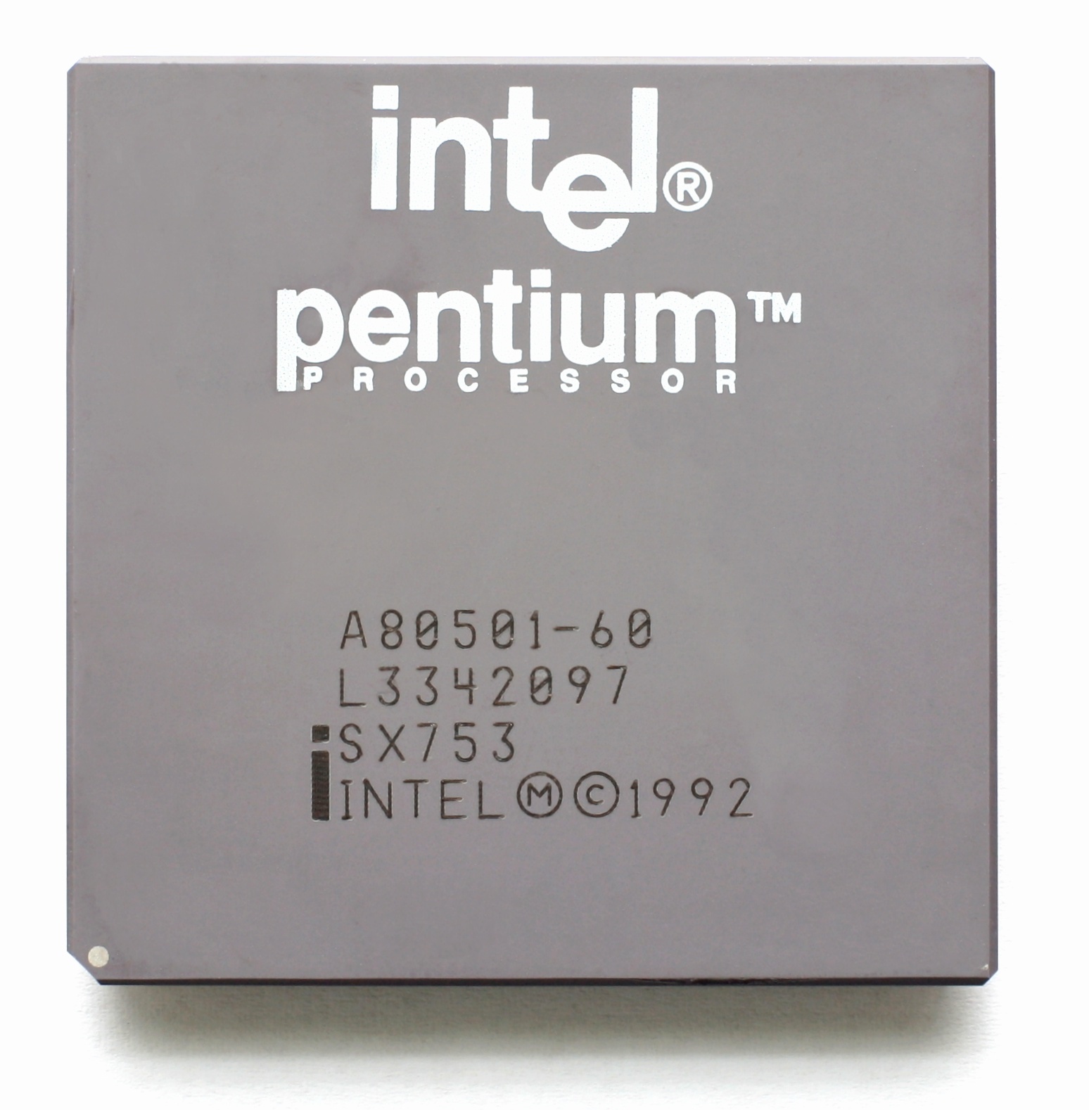 The first Intel Pentium CPU was also called P5, introduced in March 1993. For over a year there would be only two versions: 60 MHz and 66 MHz. These used the existing Socket 4 standard and ran at 5 volts.
In October 1995, Intel released the P54C range, also called "Pentium-S", which came in 75, 90 and 100 MHz versions. Crucially though, the core voltage was dropped to 3.3V which reduced energy consumption and heat (a big problem with the P5 chips). Another important change was that the P54C chips had an internal clock multiplier, so that the internal circuitry could work at a higher frequency than the external address and data buses.
Other versions followed based on the P54C design, with clock speeds up to 200 MHz.
Typical SpeedSys Score: 55 (Pentium 75), 66 (Pentium 90), 89 (Pentium 120)
Data sheets: Pentium 75-120 MHz (Mar 1995), Pentium 75-200 MHz (Jun 1997), Pentium and Pentium Pro Processors and Related Products (1996), Pentium Processor User Manual Vol. 1 (1995), Pentium Processor User Manual Vol. 2 (1995), Pentium Processor User Manual Vol. 3 (1995), Pentium Processors and Related Components (1995), Pentium Processor Specification Update (Mar 1995)
Programming: Pentium Processor Family Developers Manual Vol. 1 (Jul 1995), Pentium Processor Family Developers Manual Vol. 2 (Jul 1995)
AMD K5
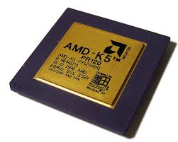 The K5 was AMD's very first microprocessor fully designed in-house. First announced in late 1994, it was aimed to compete with the Intel Pentium. During the design phase, AMD suffered significant delays, so units didn't ship until March 1996 (a whole 3 years after Intel).
The K5 had various technical improvements over the Pentium - it was closer to the 6th generation x86 CPUs like Pentium Pro - including its ability to remap CISC instructions into RISC ones for faster execution. It has 5 integer execution units and 1 floating point execution unit, and can process instructions out of order. For comparison, Pentium (classic) has only 2 integer execution units. K5 also has twice the instruction cache size (16 KB) of the Pentium (8 KB). It has fewer compatibility problems to the Pentium than the Cyrix 6x86.
Due to the K5's superior design it was able to outperform the Pentium clock for clock at integer operations, even at a lower clock speed, only being finally toppled by the Pentium 200 MHz. For floating-point operations, it was about 25% slower than a Pentium. For this reason, AMD labelled their K5 chips with a "Pentium rating", or P-Rating, to give consumers an idea of how each of their chips compared to Intel's equivalents.
Due to the K5 arriving about a year late, it was pitched as a Pentium "clone" rather than a Pentium "beater", just like Cyrix was doing with their 6x86, and of course it was sold at a significantly lower price point than the Pentium. Whilst it doesn't have the same problems with heat as the 6x86, the lower clock speeds mean that you can get better performance out of chips like the AMD 6x86-PR200+.
 Early K5s that were produced using 500nm process were labelled "5k86". These all had an SSA/5 core (the original name for the K5 was AMD SSA/5). These K5s were:
- AMD 5K86-P75 (runs at 75 MHz)
- AMD 5K86-P90 (runs at 90 Mhz)
- AMD 5K86-P100 (runs at 100 MHz)
Sadly, these chips all suffered from dreadful FPU performance and a poor design (synthetic benchmarks showed the SSA/5 FPU to be worse than the Cyrix 6x86's unit, and most real world tests confirmed this).
Following a redesign where the core was altered, cache subsystem enhanced, and FPU given a boost, later chips were produced using a 350nm process, and were labelled "K5". These were launched in October 1996, and comprised:
- K5-PR75 (runs at 75 MHz)
- K5-PR100 (runs at 75 MHz)
- K5-PR120 (runs at 90 MHz)
- K5-PR133 (runs at 100 MHz)
In synthetic benchmark testing of these new chips, we began to see some serious competition for the Cyrix 6x86 and Intel's Pentium. The K5-PR133 performed better than the Cyrix 6x86-PR166+ while running at a clock speed that was 25% lower. The FPU still wasn't as good as the more expensive Pentium, though.
All K5s, old and new, required a 3.52V core voltage.
All K5 CPUs have 3 letters after their P-rating, e.g. "ABR". The first letter denotes the package type of the chip, the second letter shows the core and I/O voltage(s), and the third letter is its case temperature limit, as follows:
| A = 296-pin SPGA | B = 3.45 - 3.6V (3.5V) C = 3.3 - 3.465V (3.3V) F = 3.135 - 3.465V (3.3V) G = ? H = 2.86 - 3V core (2.9V), 3.3 - 3.465V I/O (3.3V) J = 2.57 - 2.84V core (2.7V), 3.3 - 3.465V I/O (3.3V) K = 2.38 - 2.63V core (2.5V), 3.3 - 3.465V I/O (3.3V) |
W = 55 deg. C Q = 60 deg. C X = 65 deg. C R = 70 deg. C Y = 75 deg. C Z = 85 deg. C |
 No K5 CPUs scale well at higher clock speeds. The fastest officially-released K5 was the PR166 running at 66 MHz x 1.75 clock multiplier = 116 MHz. This was released towards the end of the K5's life. It outperformed the Pentium 166 in integer (business) applications. Where did the odd clock speed come from? Since no motherboard on this planet supports the 1.75x clock multiplier required by the K5-PR166, AMD used an internal clock multiplier setting of 1.75x which would activate every time an external 2.5x setting was detected (on the motherboard or in the BIOS).
Overclocking with both the previous SSA/5 and later K5 was nearly impossible, since they, like the Cyrix 6x86, produce enormous amounts of heat. However many reports of successful overclocking experiences with the K5-PR166 began to emerge soon after its release. It can be taken up to 75 MHz x 1.75 and even 83 MHz x 1.75 (although this isn't stable) - in all cases you need extreme cooling and a well-ventilated case when overclocking this one! I take no responsibility for fried chips or damaged motherboards.
The K5 also has an undocumented multiplier setting. If you set it to 3x it runs at 2x. The reason I believe this was added was in anticipation of the planned but never launched K5-PR200, which was supposed to run at 133 MHz and have performance equivalent of the Pentium 200 (which also uses a multiplier of 3x on a 66 MHz FSB). The K5's internal multiplier works like this:
| Motherboard multiplier set to | Internal CPU multiplier | Processors |
|---|---|---|
| 1.5x | 1.5x | 5K86-P75 5K86-P90 5K86-P100 |
| 2.0x | 1.5x | K5-PR120 K5-PR133 |
| 2.5x | 1.75x | K5-PR166 |
| 3.0x | 2.0x | K5-PR200 (unreleased) |
The AMD K5 is not for the die hard Quake fan, and although running games on it isn't unbearable...I wouldn't recommend it, at least not without a Diamond Monster 3D.
Typical SpeedSys Score: 105 (K5-PR133).
Data sheets: AMD 5K86 Technical Reference, AMD K5 data sheet (Jan 1997), K5 Processor Performance Brief (Jul 1996), Technical Reference Manual (Nov 1996)
Cyrix 6x86
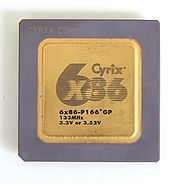 Cyrix killed off its stop-gap 5x86 after just six months so that it wouldn't tread on the toes of their brand new offering - the 6x86, also called "M1", which launched in 1996. As with their previous CPUs, Cyrix continued their relationship with chip fabrication companies including IBM and ST Microelectronics in order to manufacture their new chip, with the same rights as before so that those companies were authorised to sell their own branded variants.
The Cyrix 6x86 is not 100% instruction-set-compatible with the Intel Pentium. As such, the CPU reports itself as a 486 and has the CPUID instruction disabled. This lack of full compatibility led to some problems with certain software applications.
Furthermore, the first generation of 6x86 processors suffered from heat problems - the chips output a lot more heat than other CPUs that were readily available at the time. This meant PC manufacturers often failed to equip them with adequate cooling (a P5 Pentium outputs approximately 15W of heat compared to 25W on the 6x86). The high heat output was addressed later with the introduction of the 6x86L (the "L" stands for "low-power") which reduced power consumption by 25% or more compared to the 6x86 - this was made possible by using a new 0.35 micron manufacturing process and adding split-rail voltage (2.8V core, 3.3V I/O).
Another pitfall is that owners of 6x86 could overclock the CPU by accident by configuring the motherboard to the clock speed of the P rating instead of the actual clock speed of the chip itself! For example, a Cyrix 6x86 P133+GP has a clock of 110 MHz, but owners would see the P133 and setup their mobo for 133 MHz instead of the correct 110 MHz.
Throughout the 6x86 lifespan, Cyrix employed the "PR" performance rating or "P" rating, which they stamped on the front of the chips. The PR number (or P) relates the chip's performance relative to the Intel P5 Pentium (pre-P55C). This was because on a clock-for-clock basis the 6x86 outperformed the P5 Pentium, for example, a 133 MHz 6x86 outperforms a P5 Pentium running at 166 MHz. In such a case, the 133 MHz 6x86 would be branded "Cyrix 6x86 PR166+". The performance ratings however, are to be taken with a pinch of salt. Whilst integer performance was better on the 6x86, its floating-point performance was lacklustre.
The original 6x86 (single-voltage) CPUs were:
| Cyrix | IBM | ST |
|
|
|
| Cyrix | IBM |
|
|
The following motherboards are known to support the Cyrix 6x86L range:
- ABit IT5V, IT5H
- Antec MB5689A
- AOpen AP58, AP59S, AP5T, AP5TC, AP59 Pro, AX5T, AX5TC, MX58 Plus, MX59 Pro, MX59 Pro II
- Epox P55KTX
- Free Computer Technology P5F79
- Gigabyte GA-586ATX2
Those that support the original 6x86 are:
|
|
Data sheets: 6x86 data sheet, 6x86 Technical Brief
Cyrix 6x86MX / MII
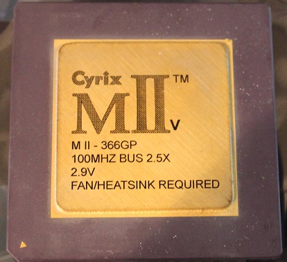 Another version of the Cyrix 6x86 was codenamed "M2" during development and upon launch in May 1997 was branded "6x86MX";
Essentially taking the Cyrix 6x86L and adding the 57 Pentium MMX instructions, these CPUs also got 4 times the internal cache size of the original 6x86 (and twice that of the Pentium MMX) at 64 KB. Initially launched in PR166, PR200 and PR233 variants using a 0.35 micron manufacturing process, these were followed later in 1997/1998 with PR250, PR266 (Mar 1998), PR300 and PR333 (both May 1998) versions. By 1999, they'd pushed clock speeds higher again with the PR333, PR350 and PR400. All 6x86MX CPUs up to and including the launch of the PR266 were manufactured at IBM's fabrication plant. Since Cyrix had been bought by National Semiconductor in November 1997, NS' own fab plant which was located in South Portland, Maine, was used from August 1998 and beyond with their 0.25 micron manufacturing process.
Another version of the Cyrix 6x86 was codenamed "M2" during development and upon launch in May 1997 was branded "6x86MX";
Essentially taking the Cyrix 6x86L and adding the 57 Pentium MMX instructions, these CPUs also got 4 times the internal cache size of the original 6x86 (and twice that of the Pentium MMX) at 64 KB. Initially launched in PR166, PR200 and PR233 variants using a 0.35 micron manufacturing process, these were followed later in 1997/1998 with PR250, PR266 (Mar 1998), PR300 and PR333 (both May 1998) versions. By 1999, they'd pushed clock speeds higher again with the PR333, PR350 and PR400. All 6x86MX CPUs up to and including the launch of the PR266 were manufactured at IBM's fabrication plant. Since Cyrix had been bought by National Semiconductor in November 1997, NS' own fab plant which was located in South Portland, Maine, was used from August 1998 and beyond with their 0.25 micron manufacturing process.
Unfortunately, Cyrix' new chip was late to market, with AMD and Intel having a few months headstart for their 6th-generation processors with MMX technology. Cyrix therefore had to bring the price down as they introduced the 6x86MX.
Cyrix changed the name of its MX processors from the PR300 and up from September 1998 onwards in order to better compete against the Intel Pentium II processor and AMD K6-II. These would be called 6x86 MII. IBM chose to retain the 6x86MX name for its branded chips. After the Cyrix brand was sold by National Semiconductor to VIA, newly manufactured MII chips were badged "MIIv".
One interesting fact about the Cyrix 6x86 design is that unlike its AMD (K6) and Intel (Pentium II) counterparts, it still performed native x86 instruction executions rather than translation into internal RISC instructions.
Watch out when configuring a system based around the 6x86MX and using the odd 83 MHz Front Side Bus speed. While this was considered fast for its time, it caused the buses to drive expansion cards way out of their design limits. PCI would be running at 41.5 MHz (compared to the more typical 33 MHz), and AGP would match the FSB speed, i.e. 83 MHz. This was often the cause of system instability. It is recommended to use 66 or 75 MHz FSB with these processors. In fact the very first 6x86MX chip was released to run at 150 MHz with a 60 MHz FSB run at a 2.x multiplier - there had been some disputes between Cyrix and IBM on whether to choose this, or run the FSB at 75 MHz with a 2x multiplier. The decision was made (partly for marketing reasons) to go with the slower 150/60 option due [again] to the 75 MHz bus speed being thought of as unusual.
Due to stability issues found in the initial 6x86MX chips, core voltage was increased from 2.8V to 2.9V, which is the same as the AMD K6-166 and K6-200.
Performance of the 6x86MX/MII is similar to the AMD K6 and Pentium II. It supports clock multipliers of 2.0x, 2.5x, 3.0x and 3.5x which cater to FSB speeds of 60, 66 and 75 MHz. Sadly since it still has the 6x86 core, its floating point performance lags behind the competition, making it a poor choice for gaming or applications that make heavy use of floating point calculations. What somewhat offsets this poor FPU is the huge 64 KB L1 cache.
Typical SpeedSys Scores: 119 (MII 166), 144 (MII 200), 166 (MII 233), 179 (MII 250), 190 (MII 266), 214 (MII 300), 238 (MII 333), 251 (MII 350), 287 (MII 400)
Data sheets: MII Data Book (Apr 1998)
Intel Pentium MMX
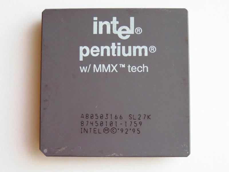 In late 1996, Intel launched the successor to the P54C - the P55C, also called Pentium MMX. The "MMX" or "MultiMedia eXtensions", was a new set of 57 instructions designed to improve multimedia performance, such as encoding and decoding digital media data.
Internally it also got lots of upgrades when compared to the P5 and P54C design, including a 6-stage pipeline, improved instruction decoder and branch predictor, and double the L1 cache size (now 32 KB).
The MMX was the first CPU to require two separate voltages from the motherboard, called "split rail" voltage - one for the core and a second for I/O. For this reason, whilst the Pentium MMX is compatible with the Socket 7 motherboard specification, all boards manufactured before the MMX was launched require an upgrade kit which Intel confusingly called OverDrive - this was completely different to the 486 OverDrive processors from 1992.
Available in 166, 200 and 233 MHz versions, Pentium MMX processors typically overclock well. Most 166 and 200 MHz chips have locked multipliers, so overclocking is best done on the 233 MHz version. Front Side Bus speeds for the Pentium MMX typically are 60, 66, 75 and even 83 MHz, although RAM and PCI bus may not cope as well at 83 MHz FSB.
They are outperformed by AMD K6-2 and K6-III CPUs.
The last of the Pentium MMX range was built specifically for notebook computers, and arrived in August 1997. Codenamed Tillamook, they initially came in 166, 200 and 233 MHz variants, but there are later ones that rose as high as 366 MHz! They were Intel's first to be produced using a 0.25μm manufacturing process. These all resided on a 'card' that slotted into the notebook PC's motherboard, and on this card was also an Intel 430TX chipset and 512 KB of L2 cache.
Intel Pentium Pro
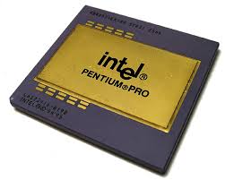 In late 1995, Intel launched what was originally to be the Pentium successor. The 'Pro' incorporated a new 'microarchitecture', different from the x86 architecture that went before it. It was primarily used in business servers and some high-end desktop PCs, but had some difficulties in running 16-bit code which was common at the time with DOS and Windows 3.1. To take full advantage of the Pentium Pro's capabilities required a full 32-bit operating system like Windows NT, Unix or OS/2. The Pro was Intel's first 6th-generation processor, so the core was called P6.
Typically the Pro was packaged on a module along with a level 2 cache which ranged from 256 KB up to 1 MB, and would reside on a Socket 8 motherboard.
Data sheets: Pentium and Pentium Pro Processors and Related Products (1996)
Programming: Pentium Pro Family Developers Manual Vol. 1 (Jan 1996), Pentium Pro Family Developers Manual Vol. 2 (Jan 1996), Pentium Pro Family Developers Manual Vol. 3 (Jan 1996)
AMD K6
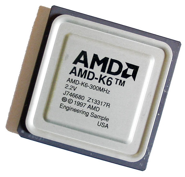 AMD's K6 processor arrived in April 1997 and was the outcome of a design by its newly acquired company, NexGen, rather than being a natural succession of the K5 core. NexGen had been working on their new chip, codenamed "NX686" when bought by AMD. Initially released in 166, 200 and 233 MHz variants in April 1997, it rocked the consumer desktop world with its performance-to-price benefits over the Intel Pentium II (it closest competitor).
Originally, the K6 was designed to use its own proprietary socket, since Intel were abandoning the Socket 7 architecture for the upcoming "Slot 1" for their Pentium II, but realised they could still leverage the now aging Socket 7 still.
By the start of 1998, AMD had moved to a 250nm production process, and launched the K6 under a new development codename, Little Foot, in new speeds from 200 MHz up to 300 MHz.
Mobile versions of the K6 were also produced for notebook computers, with speeds up to 300 MHz.
Typical SpeedSys Score: 264 (K6-233)
Data sheets: AMD K6 Data Sheet (Mar 1998), AMD K6 Revisions Guide (Aug 1998), AMD K6 Revisions Guide (Jun 1999), K6 MMX
Pentium Overdrive
 In early 1997, Intel wanted to provide a cost-effective upgrade path for those who had an original Pentium P5 CPU and motherboard. These ran at a higher voltage (5V) than later Pentium chips like the P54C.
Don't confuse these Pentium Overdrive CPUs with the earlier-released Intel Overdrive processors for the 486 family.
Pentium Overdrive processors ran with an internal clock multiplier of 2x, thus being able to run at 120 MHz or 133 MHz. These were compatible with the P5 motherboard's slower Front Side Bus of 60 or 66 MHz.
Initially, the following Overdrive CPUs were available:
- PODP5V120 - 120 MHz (on 60 MHz FSB)
- PODP5V133 - 120 MHz (on 60 MHz FSB), or 133 MHz (on 66 MHz FSB)
The price for these was around $190 in April 1997. A little later, Intel offered Pentium Overdrive CPUs for those with P54C-compatible motherboards (those with 3.3V CPU sockets) - this range comprised:
- PODP3V125 - 125 MHz (on 50 MHz FSB). Price in April 1997 was $250.
- PODP3V150 - 150 MHz (on 60 MHz FSB). Price in April 1997 was $320.
- PODP3V166 - 166 MHz (on 66 MHz FSB). Price in April 1997 was $405.
After the launch of the Pentium MMX (P55C), these were replaced with new Pentium Overdrive CPUs that also got the MMX instructions. These also got the larger L1 cache size of 32 KB, just as the Pentium MMX CPUs did:
- PODPMT60X150 - 150 MHz (on 60 MHz FSB)
- PODPMT60X180 - 180 MHz (on 60 MHz FSB)
- PODPMT66X166 - 166 MHz (on 66 MHz FSB)
- PODPMT66X200 - 200 MHz (on 66 MHz FSB)
IDT WinChip C6
 In early 1997, a new player entered the PC CPU market. IDT, who had prior experience in the RISC world, developed a simpler, cost-effective drop-in replacement for Socket 5 and Socket 7 motherboards with the WinChip C6. Competing with the Intel Pentium and Pentium MMX, Cyrix 6x86 and AMD K5 and K6, the WinChip C6 worked well in standard business applications. Its floating point performance was, however, very poor (even worse than Cyrix).
All chip variants supported MMX instructions, and came with 64 KB of L1 cache onboard. They were all designed to be low power, running at around 3.5V. Clock speeds for the first WinChip C6 series ran from 180 MHZ to 240 MHz. In 1998, IDT released the WinChip 2, which added AMD 3DNow! instructions, and clock speeds ran from 200 MHz up to 250 MHz.
Pentium II
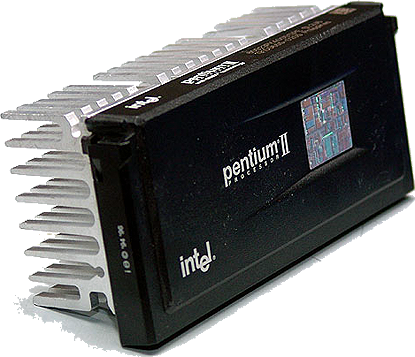 With the Pentium II, launched in May 1997, Intel took the "P6" core from their Pentium Pro microarchitecture, and made some improvements.
This was the first CPU to be incorporated on a 'card' and installed into a slot on the motherboard, rather than a socket. In a 'Slot 1', as it would be called, this processor card would also carry the level 2 cache so that the two could operate on a closely-coupled bus that was separate to the motherboard bus. With this design, Intel could compete in different markets by varying the size of the cache on its Pentium II CPU "cards".
Intel learned their lesson with poor 16-bit code compatibility on the Pro, and this was resolved on the P-II. The Pentium II also got 32 KB of on-die (level 1) cache to compensate for the slower level 2 cache.
Clock speeds started at 233 MHz and rose to 300 MHz on the initial "Klamath"-codenamed Pentium IIs. A later variant launched in January 1998 and codenamed "Deschutes", started with a 333 MHz version, and was the last Pentium II CPU that used the old 66 MHz FSB (front side bus). These got a reduced Vcore (core voltage) of 2.0V down from Klamath's 2.8V due to Deschutes being manufactured on a 0.25 micron process. This allowed clock speeds to rise without raising the core temperature to unsustainable levels. Later 100 MHz FSB versions of Deschutes were released, including 266 MHz and 300 MHz to compete in the lower markets, and 350, 400, and 450 MHz for high-end machines. With Deschutes supporting 100 MHz front side bus, Intel coincided its launch with its new 100 MHz 440BX "Seattle" chipset, along with its siblings, 440MX, 450NX and 440ZX. The 440BX chipset produced notable performance gains over 66 MHz FSB-based PCs that had been on the market since 1993.
Just as they'd done with the Pentium MMX and "Tillamook", Intel leveraged the Pentium II technology to again provide a mobile and server offering. For mobile, "Tonga" launched in April 1998, and was the same as its desktop counterpart but was produced using a 0.25μm manufacturing process. In advertising this was referred to as "Mobile Pentium II". In 1999, "Dixon" was launched, which reduced manufacturing to 0.18μm. Dixon also got a 256 KB cache on-die - these were the fastest Pentium IIs ever produced. In adverts, "Dixon"-based units were called "Mobile Pentium II PE (Performance Enhanced)".
Approximate performance of a Pentium II 350 MHz is about 5% faster than an AMD K6-2 350 MHz.
The Pentium II was superceded in 1999 with the launch of Pentium III, which was essentially just a Pentium II with SSE instructions added.
AMD K6-2 / K6-2+
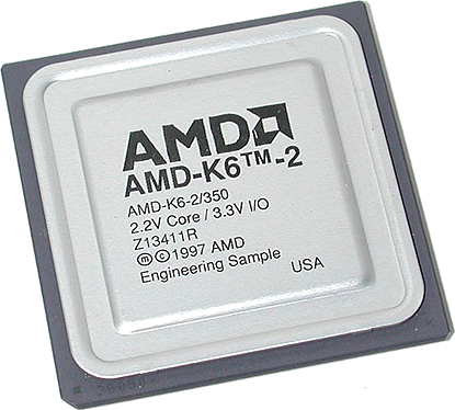 Following its success with the K6 processor in 1997, a year later AMD launched the K6-2, codenamed "Chompers". This was an enhancement over the K6 as it included new instructions dedicated to floating-point calculations, something the K6 was weak on. These were called "3DNow!", and boosted performance benchmark results significantly. Unfortunately, the 3DNow instruction set wasn't widely adopted in new applications, so the added performance wasn't often realised.
However, along with the new instruction set, the K6-2 introduced the new Super 7 bus interface which raised the processor bus speed (Front Side Bus) from 66 MHz to 100 MHz. This was backward-compatible with the older Socket 7 motherboards, so prospective customers could upgrade to a K6-2 without the added cost of purchasing a new motherboard (although the new processor would run at the slower 66 MHz bus speed). Those who adopted the new breed of Super 7 motherboards got a significant performance boost due to this higher bus speed.
The K6-2 microprocessor was manufactured using AMD's 0.25 micron process, and required a core voltage of 2.2 volts. It had no L2 cache built into its die, relying instead on the faster front side bus to carry data to and from the external L2 cache on the motherboard. They came with a huge 64KB L1 cache onboard.
At introduction the K6-2 ran at 300 MHz but later variants pushed clock speeds up to 550 MHz. It remained competitive for several years when compared to the Pentium II and also the first Celeron CPUs.
The K6-2 400 MHz, which came out in November 1998 stands out as it is the last AMD chip to be compatible with the original Socket 7 (66 MHz front-side bus) as well as the newer Super [Socket] 7 (100 MHz front-side bus) motherboards. It's also the fastest processor from any manufacturer available on the Socket 7 platform. It will happily run with a 6x multiplier on a 66 MHz bus, or 4x multiplier on a 100 MHz bus.
Typical SpeedSys Scores: 373 (K6-2/350), 455 (K6-2/400), 512 (K6-2/450), 573 (K6-2/500)
Data sheets: AMD K6-2 Data Sheet (Feb 2000), K6-2 Processor Revision Guide (Jun 1999)
K6-2+
In 2000, AMD launched the K6-2+, which despite the name was actually based on the K6-III core, but came with only half the L2 cache (128 KB) on its die. The key to its performance gains over the K6-2 was down to using a 0.18 micron CMOS process which meant it could reach higher clock speeds. It was designed to run on a FSB of 100 MHz and required a core voltage of 2.0V, though 2.1V was tolerated, and it had an absolute maximum of 2.2V, though this would no doubt shorten the lifespan of the chip.
Motherboards that did not have a Front Side Bus capable of being run at 100 MHz almost never supported the '+' CPUs, and often don't have options to set the Vcore voltage down to 2.0V or 2.1V.
Clock speeds for the K6-2+ started at 350 MHz and went up to 570 MHz.
Intel Celeron
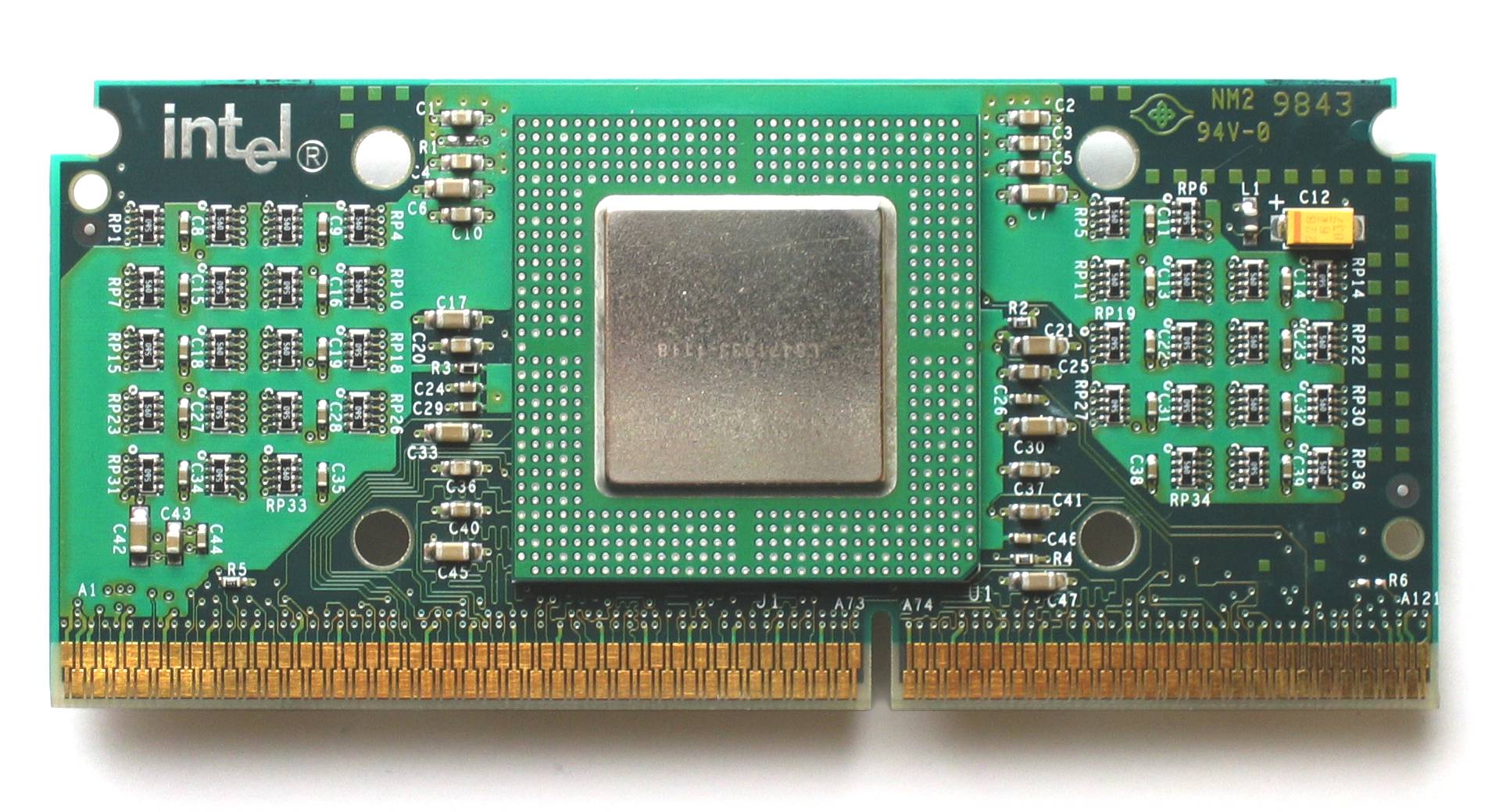 In April 1998, Intel launched a cost-effective alternative to the Pentium II. Celeron used the same Slot 1 interface for the first two variants, codenamed Covington and Mendocino.
Covington was basically a Pentium II 266 MHz with no L2 cache on the card. Unfortunately, because of the lack of cache, performance was poor despite the cheaper price tag, and Celeron's got a bad name in the press.
In reaction to this, "Mendocino" was released in August 1998. It was the first CPU to feature an "on die" level 2 cache - in Mendocino, this was 128 KB because it was on-die, it ran at the same speed as the CPU. So good were the first Mendocino Celerons, they caused a problem for Intel as buyers were moving away from Pentium II and going for Celeron due to the minimal performance hit and much more attractive cost! The first Mendocino was clocked at 300 MHz, and it had almost twice the performance of the Covington clock-for-clock! You can easily identify a Mendocino 300 MHz Celeron, as the CPU is branded as Celeron-A, though this designation is not obvious for later Mendocinos.
AMD K6-III
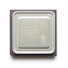 In early 1999, AMD launched the successor to the K6-2 - the K6-III (codenamed Sharptooth). Initially offered in both 400 and 450 MHz variants, it was essentially a K6-2 with an on-die L2 cache which ran at the same clock speed as the rest of the CPU.
Because of this, the K6-III was not only able to beat the Pentium II clock for clock, but also Intel's new Pentium III "Katmai" which was released just days after the K6-III. Intel wouldn't produce a CPU with an on-die cache until the launch of the Pentium III "Coppermine" CPU in October 1999. This coincided with AMD stopping production of the K6-III to focus their manufacturing on the new Athlon.
AMD were also able to sell the K6-III at a lower price point than Intel's Pentium III so these were considered a better value for money, especially when coupled with a motherboard that had a L3 cache which could be anywhere from 512 KB up to 2 MB.
The K6-III also got the new "Enhanced 3DNow!" instructions, but didn't include the new 19 extended MMX instructions
Pentium III
 Intel launched the Pentium III days after AMD launched the K6-III, in February 1999. The P-III can be considered a Pentium II with the addition of the SSE instruction set.
The initial set of P-IIIs, codenamed Katmai, were based on a 0.25um process, continued to use the Pentium II's Slot 1 interface, and started at 450 MHz rising to 600 MHz.
In October 1999 Intel released Pentium III Coppermine, which used a 0.18um manufacturing process. These were available initially only in Slot 1 form, but later moved to the new Socket 370 platform. Clock speeds rose dramatically due to the smaller manufacturing process, thus reducing heat, with 500 MHz up to 1133 MHz variants.
Later, in March 2000, Intel took the P-III Coppermine core, halved its L2 cache (thus codenamed Coppermine-128) and called it a Celeron II. These got the benefit of the Coppermine's 256-bit L2 cache bus width compared to the 64-bit width of [Celeron] Mendicino as well as Pentium II designs, but had the same cache size as the Mendocino. These were all packaged for socket 370 use, so this spelled the end for Slot 1. Coppermine-128s ran up to 1100 MHz.
The final variant of Pentium III was codenamed Tualatin, launched in 2001. It was only made for Socket 370, and brought clock speeds up to 1400 MHz. It operated on a FSB speed of 133 MHz, like some of the later Coppermine ones. Tualatins went up to 1.4 GHz clock speed.
AMD K6-2+ and K6-III+
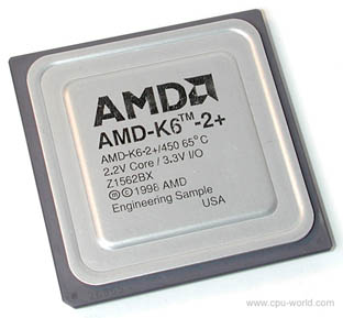 In early 1999, AMD realised they needed to make some changes to their K6 processor line to remain competitive against the Intel CPUs that were being announced. Their answer was the '+' series of processors that would sit alongside both their existing K6-2 and K6-III series.
The K6-2+ and K6-III+ microprocessors were manufactured using AMD's 0.18 micron process, and as such were designed to be low power 'mobile' CPUs which required a core voltage of 2.0 volts. AMD were still struggling in the desktop PC market to get traction with the new Athlon processor, so the '+' processors were positioned for the OEM mobile market.
The reduction in manufacturing process and voltage meant the new '+' processors produced less heat at the same clock speed when compared to their 0.25 micron siblings, as thus they could run at increased clock speeds - the K6-III+ went up to 550 MHz compared to 450 MHz for the K6-III. With the K6-2+, AMD limited the clock speed to the same as the K6-2 (up to 550 MHz). Furthermore, AMD incorporated a new technology in the '+' series - "PowerNow" - which allowed the processor to dynamically adjust its clock speed based on demand.
Another reason for the reduction in manufacturing process was that the CPU's die size was reduced so it used less silicon that the K6-2 and K6-III. This reduced the cost to manufacture the chips so AMD could be more competitive on price.
The AMD K6-2+ came with 128 KB of L2 cache built-in (the K6-2 got none), and the K6-III+ came with 256 KB of L2 cache.
Most motherboard manufacturers that supported the K6-2+ limited the clock multiplier to 5.5, since the fastest K6-2+ was 550 MHz (100 MHz front-side bus speed x 5.5 = 550 MHz). Having said that, the K6-2+ had a little-known quirk in that it interpreted a motherboard's clock multiplier settings of 2 as 6. This allowed many users to run their K6-2+ with a 6x multiplier resulting in a final clock speed of 600 MHz!