 Elitegroup Computer Systems
Elitegroup was a manufacturer of motherboards and graphics cards for the IBM PC and its compatibles during the DOS era.
They discontinued their peripheral card division in around 1999, focussing instead on motherboards.
Elitegroup Computer Systems, Co., Ltd. resided at No. 1, Lane 159, Li Teh Road, Peitou,Taipei, Taiwan, R.O.C., Tel: 886-2-896-5859, Fax: 886-2-895-1294, Web Site: www.ecs.com.tw
In the USA, Elitegroup Computer Systems, Inc. resided at 45401 Research Ave., Fremont, CA 94539, Tel: (510) 226-7333, Fax: (510) 226-7350, Site: www.ecsusa.com
Motherboards
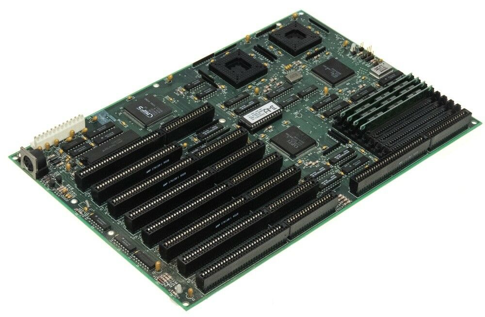
ECS-386/32
|
||||||||||
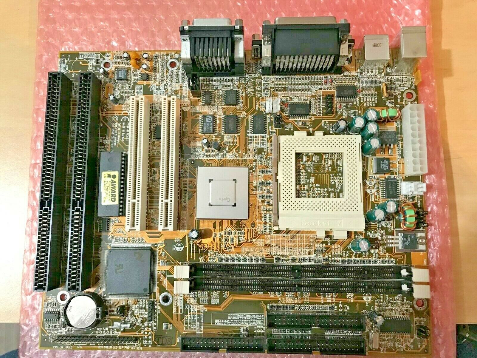
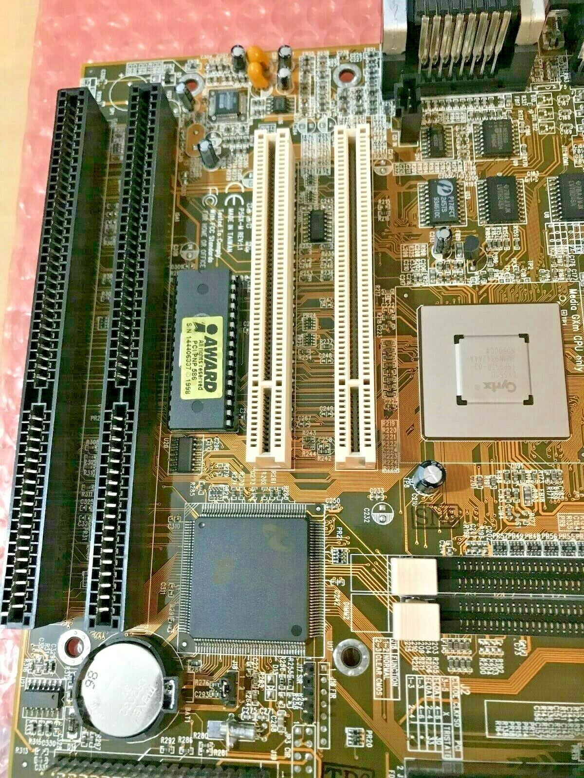
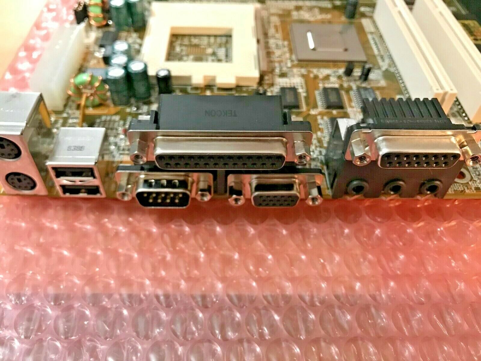
P5GX-M
Supports *only* the Cyrix/National Semiconductor MediaGXm CPU running at 200, 233 or 266 MHz.
|
||||||||||
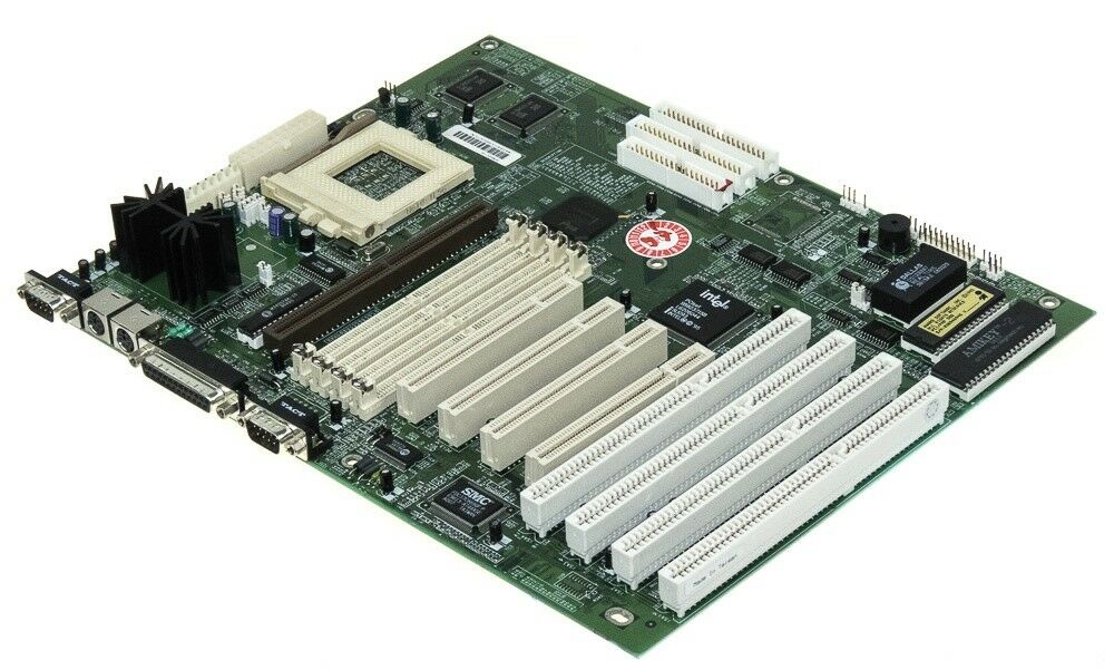
P5HX-A
Supports Intel Pentium, Pentium MMX, AMD K5 and K6, and also works with Cyrix 6x86 CPUs from P120+ up to P166. The memory slots will take either FPM or EDO RAM. The board also has a COAST slot for adding L2 cache. |
||||||||||
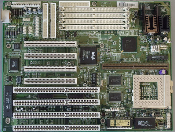
P5HX-B
Supports Intel Pentium and MMX (75 MHz up to 200 MHz), AMD K5 and K6, and also works with Cyrix 6x86 CPUs from P120+ up to P166. The memory slots will take either FPM or EDO RAM. The board also has a COAST slot for adding up to 256 KB more of L2 cache (on top of 256 KB on the mainboard itself). Jumpers JP15 and JP16 tell the board how much cache you have installed. FSB speeds can be set to either 50, 60 or 66 MHz. | ||||||||||
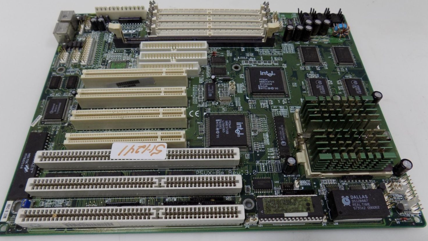
P5VX-A
|
||||||||||
P5VX-BE
|
||||||||||
UL486
|
||||||||||
UM486V AIO / AIO(DIP)
|
||||||||||
UM8810P AIO
|
||||||||||
SI54P-AIO
|
||||||||||
TSI54P-AIO
|
||||||||||
TR5510
|
||||||||||
SI5PI-AIO
|


| Hercules Dynamite 128 | 53 MB/sec |
| Matrox Millennium (MGA2064) | 52 MB/sec |
| Elsa Winner 1000 (S3 Trio64V+) | 52 MB/sec |
| S3 ViRGE 325 (4 MB) | 22.5 MB/sec |
| Tseng Labs ET6000 | 48 MB/sec |
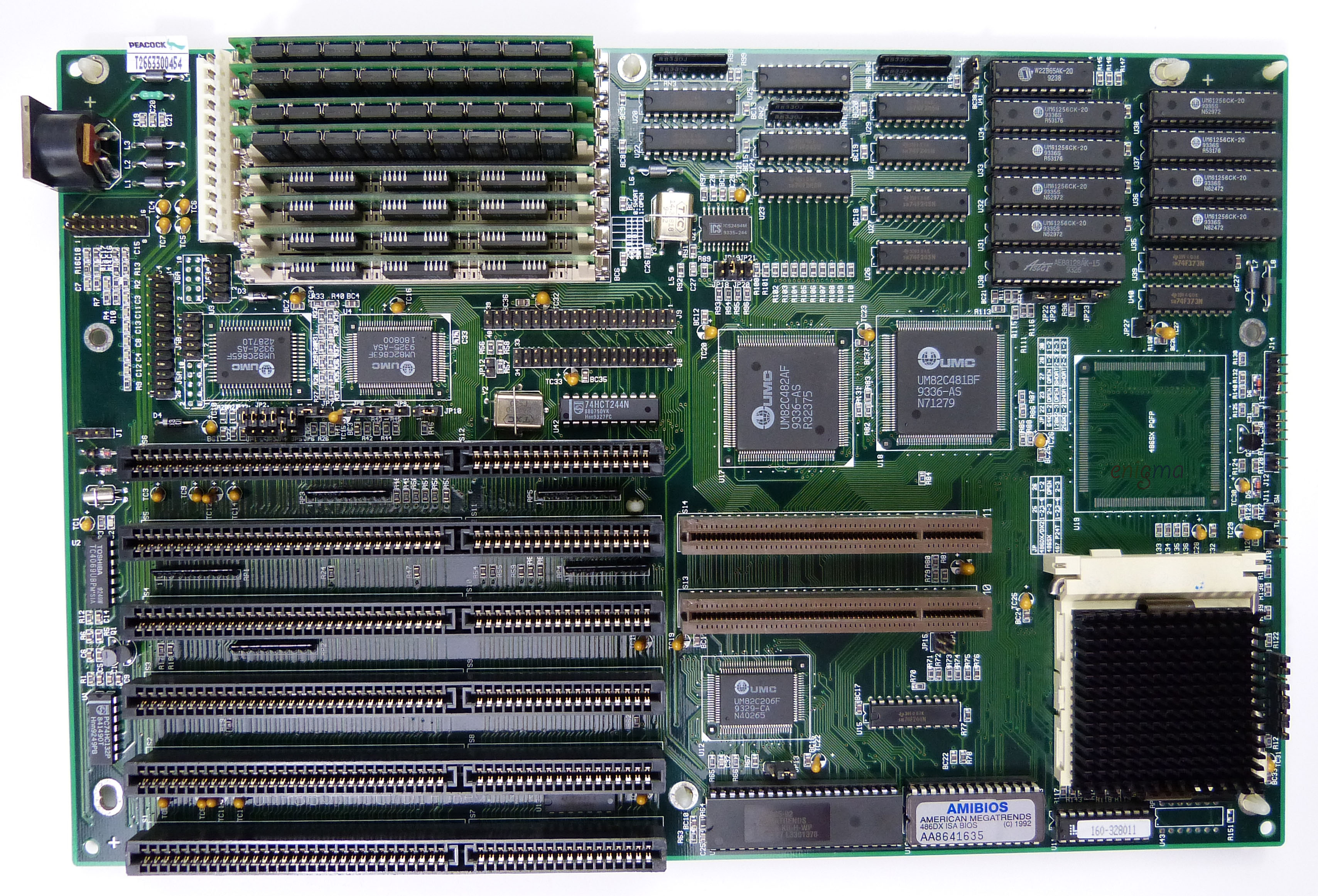
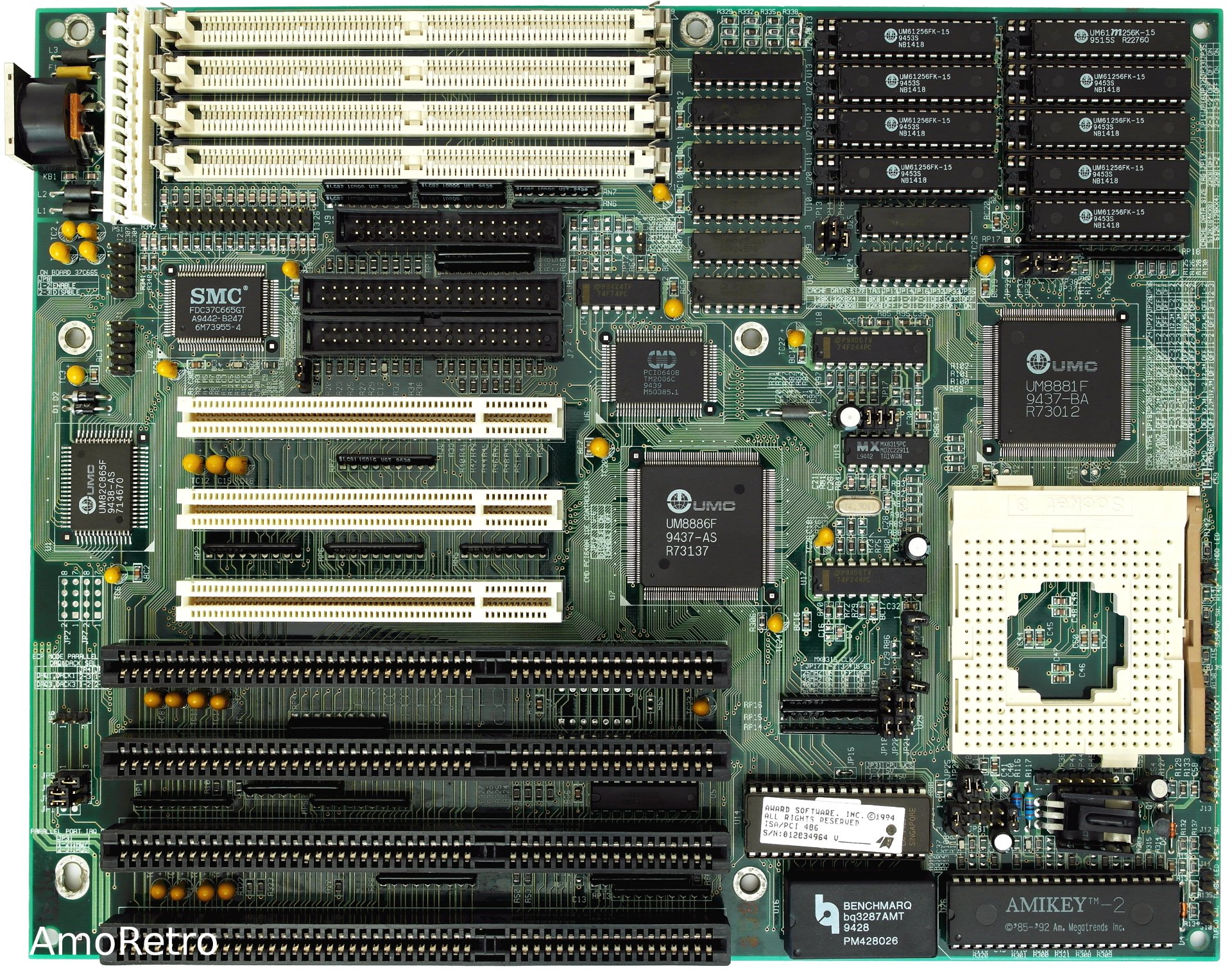
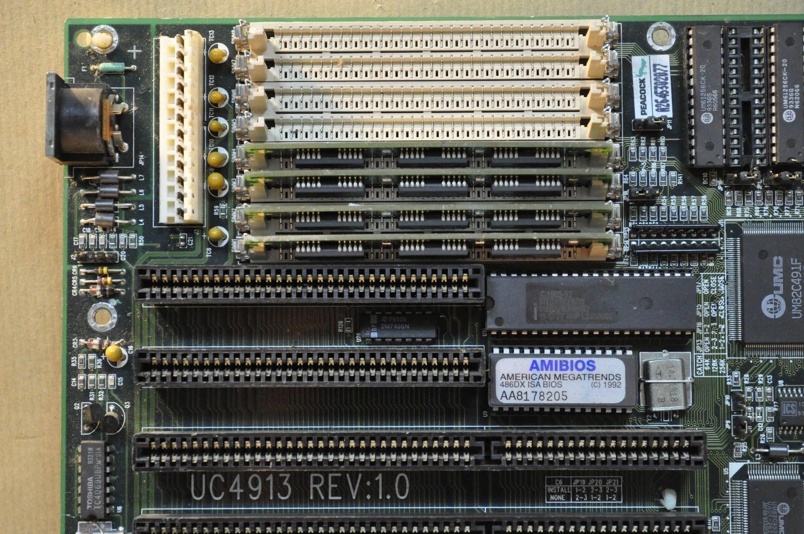
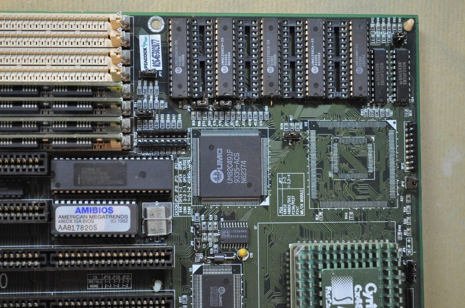
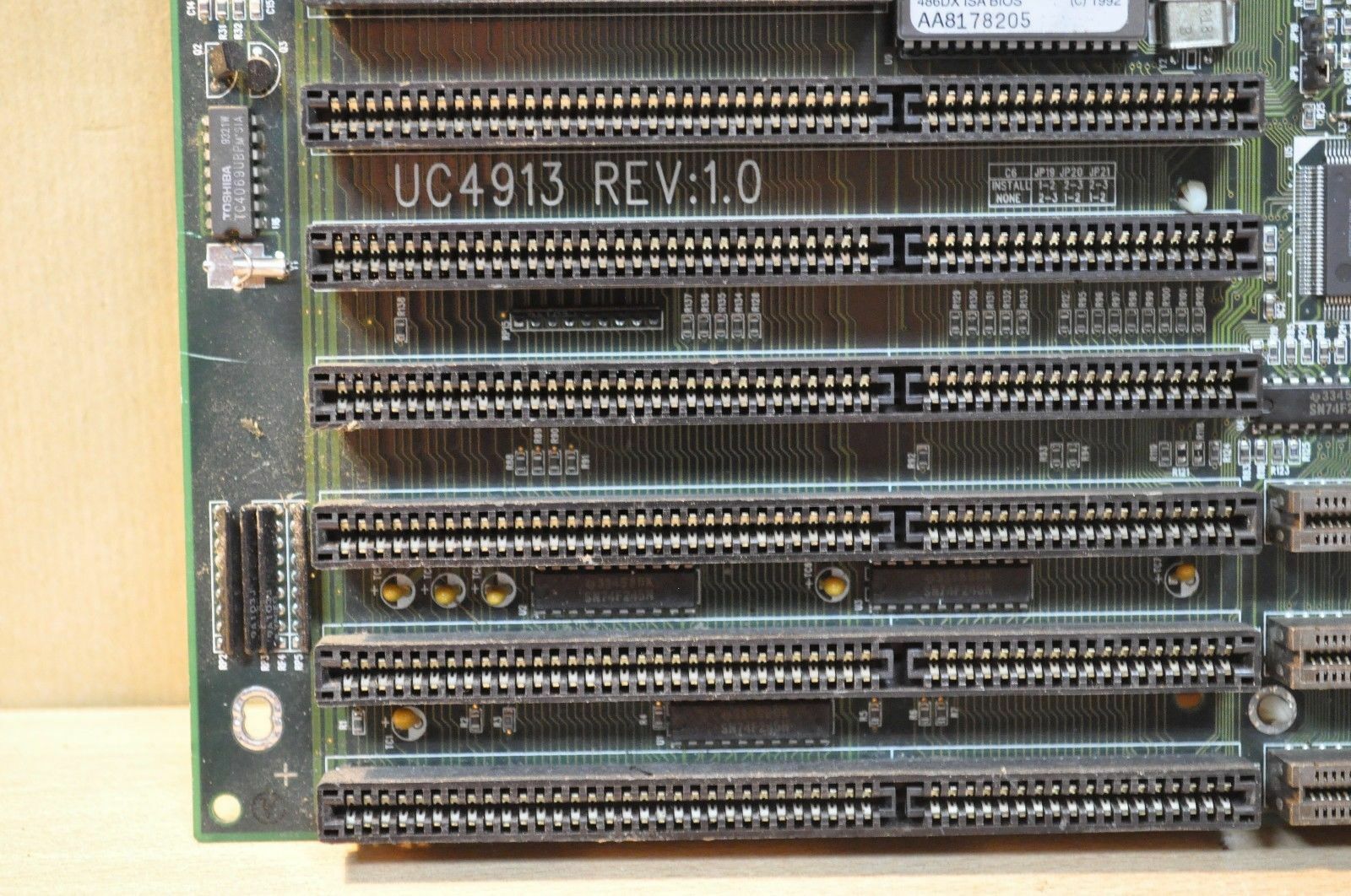
 UC4913
Year: 1992
Type: Socket 3
Form Factor: Baby AT
Power Connector: AT
Chipset: UMC UM82C491F
Slots: 2 x ISA (8-bit), 6 x ISA (16-bit), 3 x VLB
Memory: 8 x 30-pin SIMMs (2 banks)
BIOS: AMI
Known Revisions: 1.0
This board supports 486SX, 486DX, 486DX2, 4867SX (P23N), 486 Overdrive (P23T), Pentium Overdrive (P24T), and Cyrix Cx486 (M6) and IDT Winchip C6.
More Images

Graphics Cards
|
||||||||||||||||||||
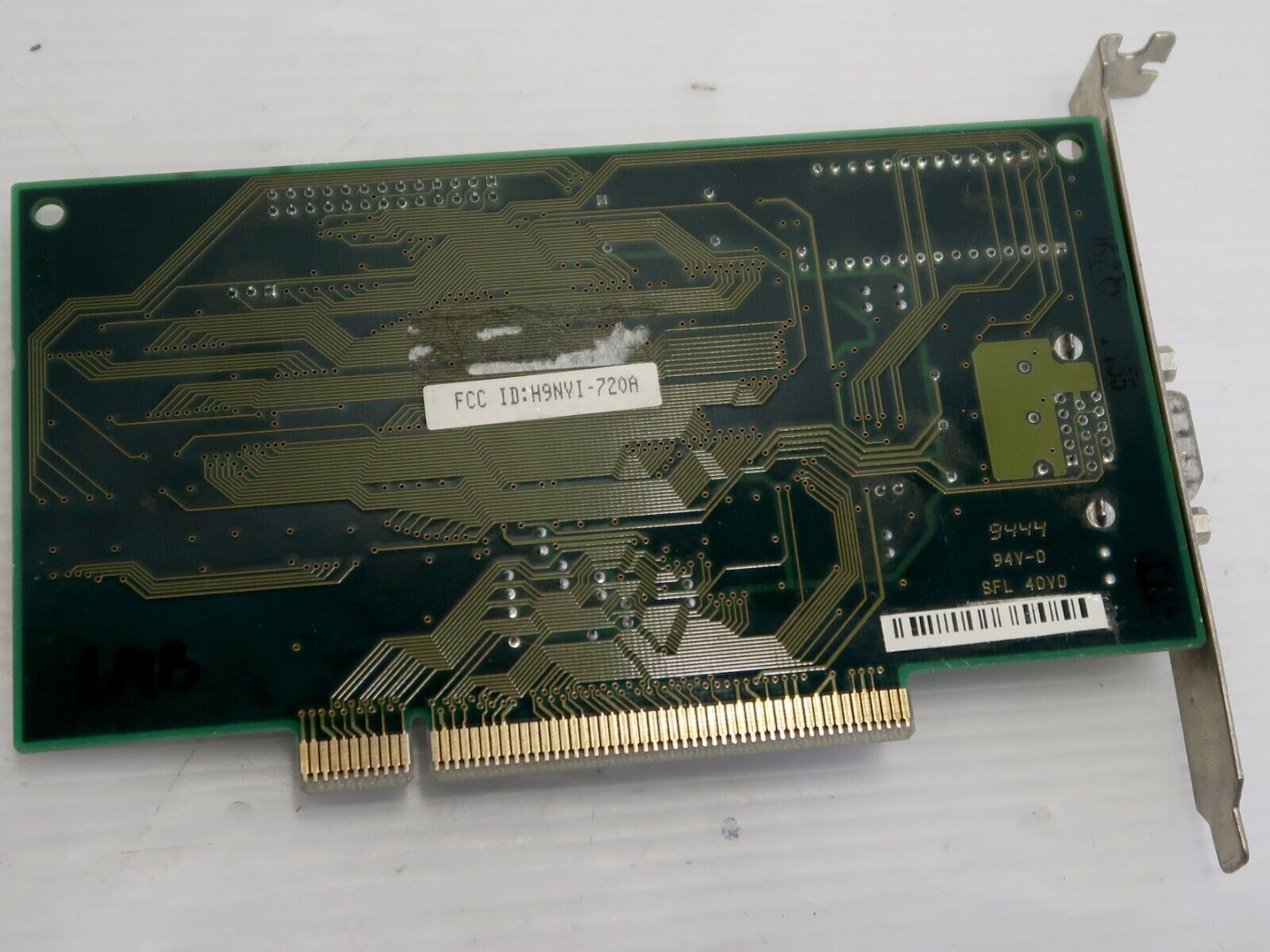
VideoImage VI-710 / VI-710A / VI-711Year: 1993? |
||||||||||||||||||||
|
||||||||||||||||||||
|
||||||||||||||||||||
|
||||||||||||||||||||
|
||||||||||||||||||||
|
||||||||||||||||||||
|
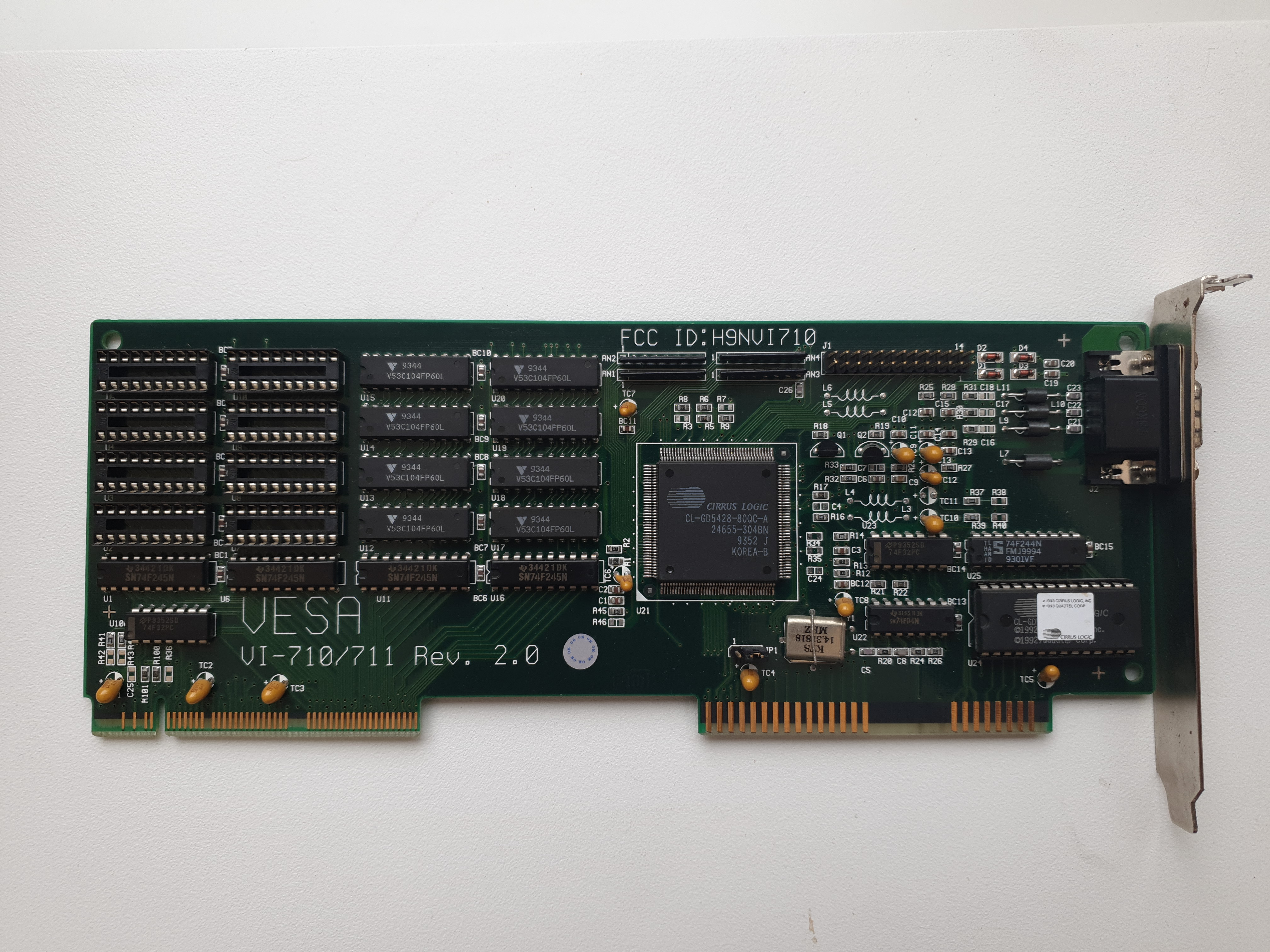
| Resolution | Display Memory |
| 1600x1200x16/256 colors | 2M |
| 1280x1024x16/256 colors, NI | 2M |
| 1024x768x64K colors | 2M |
| 800x600x64K colors | 2M |
| 1024x768x16/256 colors | 1M |
| 800x600x16/256 colors | 1M |
| 640x480x16/256/64K/16.8 million colors | 1M |
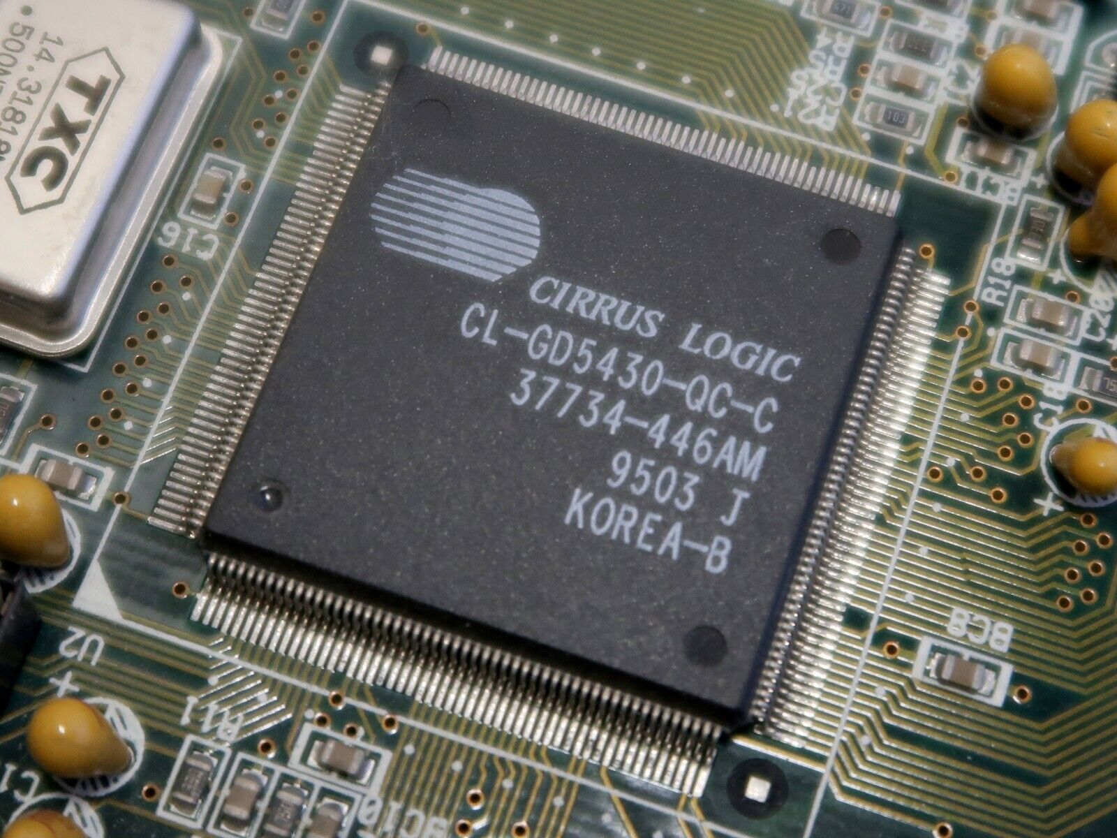
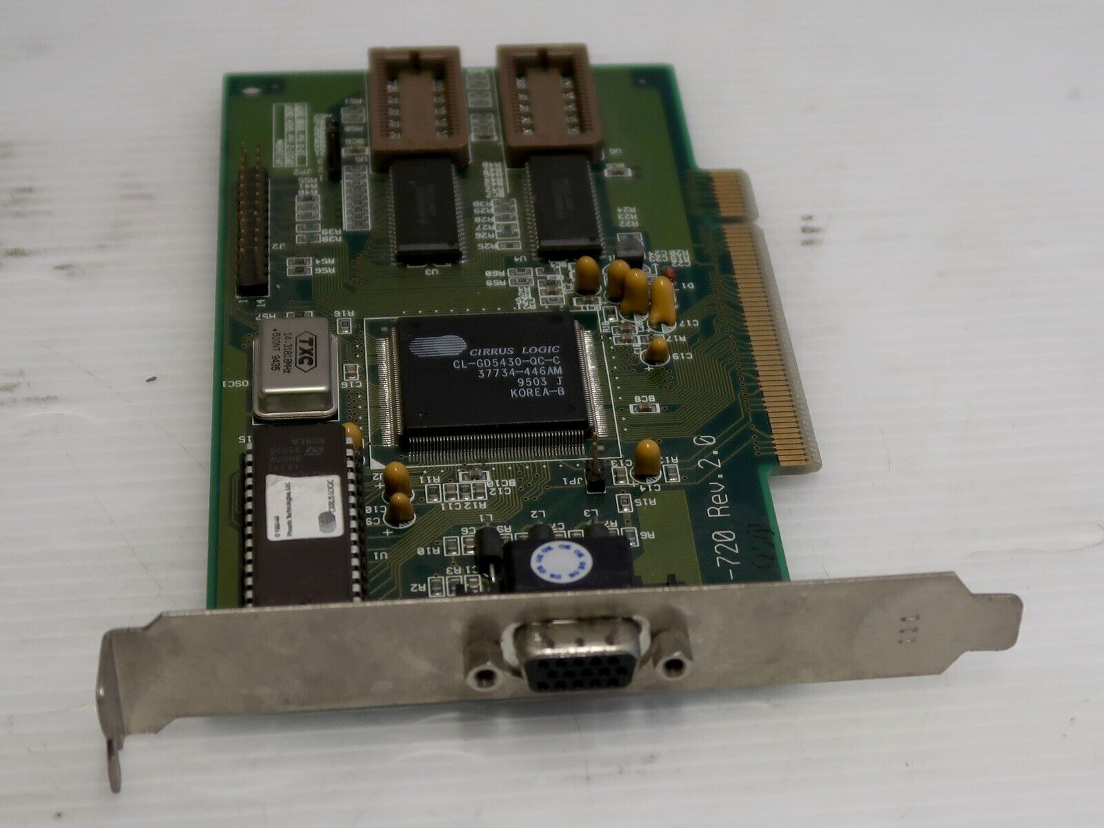
 VideoImage VI-940A / VI-940B
Year: 1995?
Type: PCI
Chipset: S3 Trio32 (VI-940A) or S3 Trio64 (VI-940B)
Memory: 4 MB?
FCC ID: -
Known Board Revisions: -
VideoImage VI-941 / VI-941A / VI-941B
Year: 1995
Type: PCI
Chipset: S3 Trio32 (VI-941A) or S3 Trio64 (VI-941B)
Memory: 1 MB or 2 MB DRAM
FCC ID: -
Known Board Revisions: -
VI-941 is a cost effective PCI graphic card using S3 Trio series GUI accelerator. The VI-941A is installed with Trio32 (32-bit GUI accelerator) controller, and the VI-941B is Trio64 (64-bit GUI accelerator). The VI-941A supports up to 1MB DRAM for the 32-bit memory interface architecture. The VI-941B supports 1MB DRAM on board, maximum to 2MB.
Bus Interface
- Compatible with PCI 2.0 standard
Display Interface:
- Features
- Resolution supports up to 1600x1200 256 colors
- Supports 32/64-bit memory interface
- Supports for Display Power Management Signaling (DPMS) in ROM
- Display DRAM
VI-941A: Supports 1MB DRAM on board only - you can upgrade to 2 MB, but no more hi-resolution mode and performance enhancement.
VI-941B: Supports 1MB DRAM (8 pcs of 256Kx4) on board, 2MB optional (2 pcs of 256K x16).
Key Components:
- Trio64/Trio32 : S3 PCI bus GUI accelerator
- Pin-compatible S3 Trio64 (64-bit Graphics Engine) and Trio32 (32-bit Graphics Engine)
- Integrated 24-bit RAMDAC and Programmable Dual-clock Synthesizer
- Extensive Static/Dynamic Power Savings
- DDC Monitor Communications Support
- 208-pin PQFP
VGA Modes Supported:
| Resolution | Display Memory |
|---|---|
| 1600x1200x16/256 colors | 2M |
| 1280x1024x16/256 colors, NI | 2M |
| 1024x768x64K colors | 2M |
| 800x600x64K/16.8 million colors | 2M |
| 1024x768x16/256 colors | 1M |
| 800x600x16/256 colors | 1M |
| 640x480x16/256/64K/16.8 million colors | 1M |
VideoImage VI-942
Year: January 1996
Type: PCI
Chipset: S3 Trio64V+
Memory: 1 MB, 2 MB or 4 MB
FCC ID: -
Known Board Revisions: -
The VI-942 64-bit DRAM-based multimedia graphic card provides accelerated graphics and video, high resolutions, true color and multimedia capabilities. It is installed with S3 Trio64V+ graphic and video accelerator and designed with DRAM up to 2 MB.
The VI-942 supports a video engine for video playback decompression algorithms. Its integrated color space conversion, scaling and dithering further enhance the user interface and increase video performance.
For low power consumption (Green PC), the VI-942 allows software manipulation of its horizontal and vertical sync signals to control the power state of monitors. The VI-942 also supports the VESA Display Data Channel (DDC1 and DDC2) standard that permits transfer of monitor identification and resolution support data.
Bus Interface
- Compatible with PCI 2.0 standard
- VI-942 Rev1.0: Only supports software MPEG
- VI-942 Rev2.0: Supports Local Peripher Bus (LPB) for Hardware MPEG Daughter board (LPB-100) or connect to other LPB device
Display Interface
- Features
- 64-bit graphic engine and video interface
- Supports 64-bit memory interface
- Supports for Display Power Management Signaling (DPMS) in ROM
- Video Playback
- Software MPEG
- Display DRAM
- Supports 1MB DRAM (8 pcs of 256Kx4) on board, 2MB optional (2 pcs of 256Kx16)
Key Components :
- Trio64V+ :
- Integrated 135MHz, 24-bit RAMDAC and Programmable Dual-clock Synthesizer
- High quality hardware assisted video playback
- Full hardware and BIOS support for VESA Display Power Management Signaling (DPMS) monitor power savings modes
- Industry Standard 208-pin PQFP package
- Support for Indeo Cinepak, and software accelerated MPEG-1 video playback
VGA Modes Supported:
| Resolution | Display Memory |
| 1600x1200x16/256 colors | 2MB |
| 1280x1024x256 colors | 2MB |
| 1024x768x64K colors | 2MB |
| 800x600x64K/16.8 million colors | 2MB |
| 1600x1200x16 color | 1MB |
| 1280x1024x16 colors | 1MB |
| 1024x768x16/256 colors | 1MB |
| 800x600x16/256 colors | 1MB |
| 640x480x16/256/64K/16.8 million colors | 1MB |
3DVision-6326
Year: 1997
Type: AGP 2x
Chipset: SiS 6326
Memory: 4 MB EDO SDRAM
RAMDAC Speed: 175 MHz
FCC ID: -
Known Board Revisions: -
The 3DVision-6326 was based on the SiS 6326 graphics accelerator chipset, and came with a TV-Out port. I was able to provide a screen resolution up to 1280 x 1024 in 24-bit colour depths at an 85 Hz refresh rate.
AG305-32
Year: 199x
Type: AGP 2x
Chipset: SiS 305
Memory: 32 MB SDRAM
The AG305-32 was a 128-bit 2D graphics accelerator with a 128-bit 3D graphics engine combined with a 24-bit True Color RAMDAC. It ran with a 270 MHz core clock and offered display resolutions up to 1920x1440 in 256 colours at 60 Hz non-interlaced.
AG315-E32
Year: 199x
Type: AGP 4x
Chipset: SiS 315E
Memory: 32 MB SDRAM
The AG315-E32 was a 256-bit 3D graphics accelerator combined with a 24-bit True Color RAMDAC. It ran with a 375 MHz core clock and offered display resolutions up to 2048x1536 in 256 colours. The SiS chip also had a DVD Dynamic Compensation Decoder video accelerator for multimedia application. It was compatible with DirectX 8.