Motherboard Chipsets
A wide variety of PC chipsets were released over the years, and they came in various levels of performance, quality and compatibility. Chipsets really began during the 286 era and became more and more of a crucial choice among PC buyers as technology improved with faster memory performance, faster CPUs and faster buses.
What is a Chipset?
Chipsets was a means of reducing the component count on a motherboard, and hence reduce the cost to manufacture. Early PC motherboards had potentially over 100 discrete electronic components (resisters, capacitors, transistors, diodes, etc) which made the board physically very large and prone to reliability problems. With the introduction of VLSI (Very Large-Scale Integration) and advancements in the design and manufacturing of ICs (Integrated Circuits), most of this logic could be condensed into much fewer, more complex, chips. We called these chipsets. Some early examples in the PC world were from Chips & Technologies, where up to 7 chips were grouped into a chipset in order to provide the motherboard with most of its functionality, such as memory addressing, controlling the bus, managing peripherals, etc.
For a list of all the chipset manufacturers I have information on at DOS Days, including everything pre-486 era, head over to the Hardware Index page and select a manufacturer under the 'Chipsets' heading.
The rest of this page provides some information on many of the chipsets seen during the 486 era. The following chart contains my own personal opinions of which chipsets, broadly speaking, are good, average or poor, and in no way reflect the thoughts and opinions of others.
| Manufacturer | Opinion | Comments |
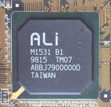
| ALI | Good | ALI made the best chipsets, hands-down. One that wasn't so good was the ALi MAGiK 1 for Athlon CPUs. |
| Intel | Good | 430HX was very stable. 430FX was slow. 440BX was a long-running favourite through the Super Socket 7 era with its introduction of supporting 100 MHz Front-Side Bus and AGP. Intel 810 and 815 had a 512MB RAM limit, and the 815 / 820's had many reports of issues. |
| nVidia | Average | nForce 2, 680i, 750i and nForce 3 often suffered from compatibility and/or stability issues. nForce4 coupled with Socket 939 AMD boards were very stable. |
| ATI | Average | Made some chipsets during the Pentium 4 era that weren't good. |
| AMD | Average | AMD 761 is a good chipset. 640 is just a clone of the VIA Apollo VP2. |
| SiS | Poor | Typically paired with budget motherboards. Most are considered a poor choice due to limited overclocking features. Some stability problems. SiS 735 not bad - fast and cheap. |
| VIA | Poor | Fairly ok Apollo MVP3 chipset, and the KT600 wasn't bad. Others like the Apollo Pro 133, VXPro, KT133/KX133 and KT400 had huge issues with their device drivers, AGP support, and poor memory compatibility. |
Quick Index
| M1429 | 430LX Mercury | 440EX | 450KX Mars | 407 / 471 | VP1 Apollo 1 |
| M1439 | 430NX Neptune | 440BX Seattle | 450GX Orion | 496 / 497 | VP2 / Apollo VP2/97 |
| M1489 | 430FX Triton | 440FX Natoma | 5571 | VPX / Apollo VPX/97 | |
| Aladdin III | 430MX | 440GX | 810 | 5591 | VP3 / Apollo VP3 |
| TXPro Aladdin IV | 430HX Triton II | 440LX Balboa | 810e | 530 / 5595 | MVP3 / Apollo Mobile VP3 |
| Aladdin V | 430TX | 440MX Banister | 815/815e | 5596 | MVP4 |
| 430VX Triton III/VX | 440NX | 820 | 540 | Apollo Pro | |
| 440ZX | 5597/5598 | VXPro / VXPro+ | |||
| 640 | 630 | ||||
| nForce 680i | |||||
| nForce 750i |
 AMD 640 Chipset
This was an officially licensed VIA Technologies' Apollo VP2/97 chipset, and branded AMD. It supported AMD K6 and Cyrix 6x86 CPUs.
Example AMD 640 chipset motherboards:
Shuttle HOT-603 (Socket 7 AT)
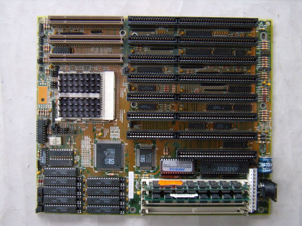
SiS 85C407 / 85C471 Chipset
This was a 486 chipset, sometimes found on motherboards with EISA and VLB slots.
| Common Name | SiS 85C407 / 85C471 | |
| Chipset Packaging | Number of chips | 2 |
| Packaging Type | Unknown | |
| CPU Support | Number of CPUs | 1 |
| AMD CPUs Supported | AMD486DX/DX2/DXL | |
| Cyrix CPUs Supported | CX486DX/DX2 | |
| Intel CPUs Supported | 486SX/DX/DX2/DX4 | |
| Cache | Type | |
| Maximum Supported Size | ||
| Maximum Cacheable DRAM Area | 128KB/256KB/512KB | |
| Memory | Maximum DRAM Supported | 512MB |
| BEDO DRAM Read Timings (66MHz) | ||
| EDO DRAM Read Timings (66MHz) | ||
| FPM DRAM Read Timings (66MHz) | ||
| SDRAM Read Timings (66MHz) | ||
| Data Path to Memory | ||
| ECC Support | ||
| Hard Disk Controller | Chip | |
| Busmastering Support | ||
| UltraDMA Support | ||
| Max. Theoretical Transfer Rate | ||
| PCI Interface | Supported PCI Bus Speeds | 25, 33, 40, 50, 66MHz |
| Concurrent PCI | ||
| Async. PCI Bus Speed | ||
| PCI Specification | ||
| Power Management | PC97 Compliance | |
| Suspend to Disk | ||
| HDD Power Down | ||
| Modem Wakeup | ||
| System Suspend | ||
| Video | AGP Support | |
| Unified Memory Architecture | ||
| Peripheral Support | USB Support | |
| Plug and Play Port | ||
| Write Buffers | CPU-to-DRAM | |
| CPU-to-PCI | ||
| PCI-to-DRAM | ||
| Officially Supported Bus Speeds | 25, 33, 40, 50, 55MHz | |
| Unofficially Achieved Bus Speeds | ||
Example SiS 85C407 / 85C471 chipset motherboards:
Acer VI15G 486 VESA |
ABit AB-AG4 |
ABit AH-4T |
AIR 486MI |
AMI Super Voyager VLB-3 |
ASUS VL/I-486SV2GX4 |
ASUS VL/ISA-486SV2B |
CMC 486DX4 |
Free <Unknown Model #> |
AIR 486SH |
<Unknown Brand> S486G Green |
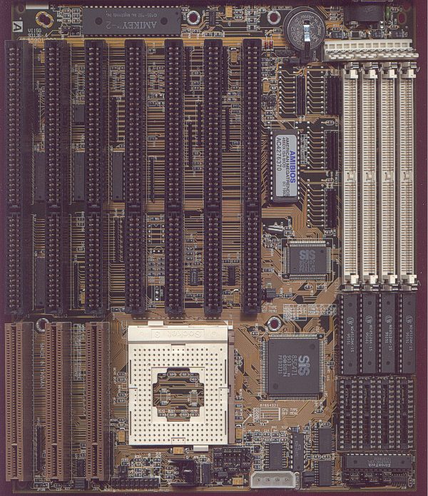


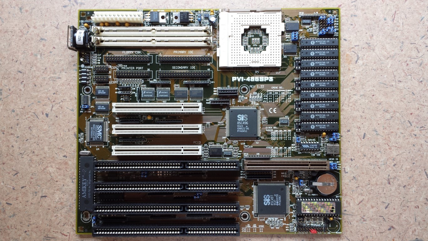
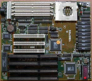
SiS 496 / 497 Chipset
This was a 486 chipset used on a number of motherboards which had a combination of ISA, PCI and VESA Local Bus capabilities. It supported all 486 CPUs including DX, SX, DX2, DX4, Overdrive, and compatibles such as the UMC U5-S and Cyrix Cx5x86, with CPU speeds ranging from 25-100 MHz. The chipsets permits FSB speeds from 25-50 MHz, and caters for up to 256 MB of FPM single-channel main memory. Mainboards that used this chipset and suitably equipped with the faster supported processors found that performance was on par with early Intel Pentium systems, and at a lower price point. The 85C496 is the Northbridge chip and the 85C497 is the Southbridge.
| Common Name | SiS 85C496 / 85C497 | |
| Chipset Packaging | Number of chips | 2 |
| Packaging Type | Unknown | |
| CPU Support | Number of CPUs | 1 |
| AMD CPUs Supported | AMD486DX/DX2/DXL | |
| Cyrix CPUs Supported | CX486DX/DX2, C5x86 | |
| Intel CPUs Supported | 486SX/DX/DX2/DX4 | |
| Cache | Type | |
| Maximum Supported Size | ||
| Maximum Cacheable DRAM Area | 128KB/256KB/512KB | |
| Memory | Maximum DRAM Supported | 256MB |
| BEDO DRAM Read Timings (66MHz) | ||
| EDO DRAM Read Timings (66MHz) | ||
| FPM DRAM Read Timings (66MHz) | ||
| SDRAM Read Timings (66MHz) | ||
| Data Path to Memory | ||
| ECC Support | ||
| Hard Disk Controller | Chip | |
| Busmastering Support | ||
| UltraDMA Support | ||
| Max. Theoretical Transfer Rate | PIO Mode 3 | |
| PCI Interface | Supported PCI Bus Speeds | 25, 33, 40, 50 MHz |
| Concurrent PCI | ||
| Async. PCI Bus Speed | ||
| PCI Specification | Yes | |
| Power Management | PC97 Compliance | |
| Suspend to Disk | ||
| HDD Power Down | ||
| Modem Wakeup | ||
| System Suspend | ||
| Video | AGP Support | |
| Unified Memory Architecture | ||
| Peripheral Support | USB Support | |
| Plug and Play Port | ||
| Write Buffers | CPU-to-DRAM | |
| CPU-to-PCI | ||
| PCI-to-DRAM | ||
| Officially Supported Bus Speeds | 25, 33, 40, 50 MHz | |
| Unofficially Achieved Bus Speeds | ||
Example SiS 85C496 / 85C497 chipset motherboards:
ASUS PVI-486SP3 |
AOpen AP43 |
Soyo SY-4SAW2 |
CMC C4PI |
Genoa / Free / Hokkins 486F55 |


Award BIOS Chipset code: 2A4IB
SiS 5571 Chipset (aka Trinity)
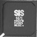 Silicon Integrated Systems, commonly known as SiS, has often been associated with one specific processor, the Cyrix 6x86 ever since MTech used it in their Mustang motherboard.
The SiS 5571, supports a maximum of 1MB of L2 cache, although to the best of my knowledge that can only cache 64MB of system RAM and currently no motherboard manufacturer has taken advantage of the 1MB L2 cache limit. The main reason for the 5571's popularity stems from its support for Linear Burst Mode, a function used in IBM/Cyrix processors for a 2.5% increase in performance.
The 5571 unfortunately doesn't support any enhanced power saving features like the Intel 430TX chipset nor support for the UltraATA hard disk specification which limit the 5571's competitive nature in today's market, however when it was released it was a sure fire "numero uno" product. It still is a great chipset, although recent contributions from VIA have proved that SiS will have to work much harder to hold onto their share of the market. The 5582 chipset by SiS may prove to recover some of the attention SiS has lost in recent times however..
| Common Name | SiS 5571 | |
| Chipset Packaging | Number of chips | Unknown |
| Packaging Type | Unknown | |
| CPU Support | Number of CPUs | 1 |
| AMD CPUs Supported | K5, K6 | |
| Cyrix CPUs Supported | 6x86 (M1), 6x86MX (M2) w/ Linear Burst Mode | |
| Intel CPUs Supported | Pentium, Pentium MMX | |
| Cache | Type | Synchronous Pipeline Burst Cache |
| Maximum Supported Size | 1024KB | |
| Maximum Cacheable DRAM Area | 64MB | |
| Memory | Maximum DRAM Supported | 384MB |
| BEDO DRAM Read Timings (66MHz) | N/A | |
| EDO DRAM Read Timings (66MHz) | 5-2-2-2 | |
| FPM DRAM Read Timings (66MHz) | 5-3-3-3 | |
| SDRAM Read Timings (66MHz) | 5-1-1-1 | |
| Data Path to Memory | 64-bits | |
| ECC Support | No | |
| Hard Disk Controller | Chip | Unknown |
| Busmastering Support | Yes | |
| UltraDMA Support | No | |
| Max. Theoretical Transfer Rate | PIO Mode 4/DMA Mode 2 (16.6MB/S) | |
| PCI Interface | Supported PCI Bus Speeds | 25, 30, 33 MHz |
| Concurrent PCI | Yes | |
| Async. PCI Bus Speed | Yes | |
| PCI Specification | 2.0 (66 MHz max.) | |
| Power Management | PC97 Compliance | No |
| Suspend to Disk | No | |
| HDD Power Down | Yes | |
| Modem Wakeup | No | |
| System Suspend | No | |
| Video | AGP Support | No |
| Unified Memory Architecture | No | |
| Peripheral Support | USB Support | Yes |
| Plug and Play Port | Yes | |
| Write Buffers | CPU-to-DRAM | 16 QWords (?) |
| CPU-to-PCI | 5 DWords (?) | |
| PCI-to-DRAM | 18 DWords (?) | |
| Officially Supported Bus Speeds | 50, 60, 66, 75 MHz | |
| Unofficially Achieved Bus Speeds | 83 MHz | |
Example SiS 5571 chipset motherboards:
Microstar MS-5147 |
M-Tech R534 |

SiS 5591 Chipset
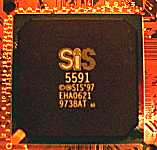 The 5591 chipset was one of the very first AGP-enabled Super Socket 7 chipsets. This chipset was seen on the MTech R581A motherboard, which whilst fully supported bus speeds of 83.3 MHz never really worked at 100 MHz with any modicum of stability.
| Common Name | SiS 5591 | |
| Chipset Packaging | Number of chips | 1 |
| Packaging Type | 1 x 480-pin BGA | |
| CPU Support | Number of CPUs | 1 |
| AMD CPUs Supported | K5, K6 | |
| Cyrix CPUs Supported | 6x86 (M1), 6x86MX (M2) w/ Linear Burst Mode | |
| Intel CPUs Supported | Pentium, Pentium MMX | |
| Cache | Type | Synchronous Pipeline Burst Cache |
| Maximum Supported Size | 384MB | |
| Maximum Cacheable DRAM Area | 256MB | |
| Memory | Maximum DRAM Supported | 384MB |
| BEDO DRAM Read Timings (66MHz) | N/A | |
| EDO DRAM Read Timings (66MHz) | 5-2-2-2 | |
| FPM DRAM Read Timings (66MHz) | 5-3-3-3 | |
| SDRAM Read Timings (66MHz) | 5-1-1-1 | |
| Data Path to Memory | 64-bits | |
| ECC Support | No | |
| Hard Disk Controller | Chip | Integrated Controller |
| Busmastering Support | Yes | |
| UltraDMA Support | Yes | |
| Max. Theoretical Transfer Rate | PIO Mode 5/DMA Mode 3 (33.3MB/S) | |
| PCI Interface | Supported PCI Bus Speeds | 25, 30, 33 MHz |
| Concurrent PCI | Yes | |
| Async. PCI Bus Speed | Yes | |
| PCI Specification | 2.1 (66 MHz max.) | |
| Power Management | PC97 Compliance | Yes |
| Suspend to Disk | Yes | |
| HDD Power Down | Yes | |
| Modem Wakeup | Yes | |
| System Suspend | Yes | |
| Video | AGP Support | Yes |
| Unified Memory Architecture | Yes (onboard VGA) | |
| Peripheral Support | USB Support | Yes |
| Plug and Play Port | Yes | |
| Write Buffers | CPU-to-DRAM | Unknown |
| CPU-to-PCI | Unknown | |
| PCI-to-DRAM | Unknown | |
| Officially Supported Bus Speeds | 50, 60, 66, 75 MHz | |
| Unofficially Achieved Bus Speeds | 83 MHz | |
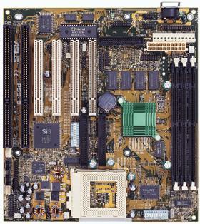
SiS 530 (Sinbad) / 5595 Chipset
This chipset provided support for up to 1.5 GB of SDRAM, FSB frequencies from 66 MHz to 124 MHz, and from 2-8 MB of shared memory for its integrated AGP SiS 6306 2D/3D graphics controller. This onboard VGA supports Direct 3D 6.0 and OpenGL, although it is considered a low-performing 3D accelerator. It was one of the first to include an integrated ATA/66 IDE controller.
This chipset was often found in low-end mainboards, coupled with non-Intel CPUs such as AMD's K6 and Cyrix 6x86.
SiS530 = Northbridge
SiS 5595 = Southbridge
Example SiS 530/5595 chipset motherboards:
Asus P5S-B |
Gigabyte GA-5SMM |
Jetway J-531CF |
SiS 540 (Spartan) Chipset
This chipset was designed for the AMD K6-III and integrates the SiS 300 graphics controller. It has exactly the same features as the SiS 630.
SiS 5596 Chipset
This chipset continued SiS' plan to keep costs low through high levels of integration. The 5596 chipset includes integrated video (onboard VGA).
SiS 5597/5598 Chipset
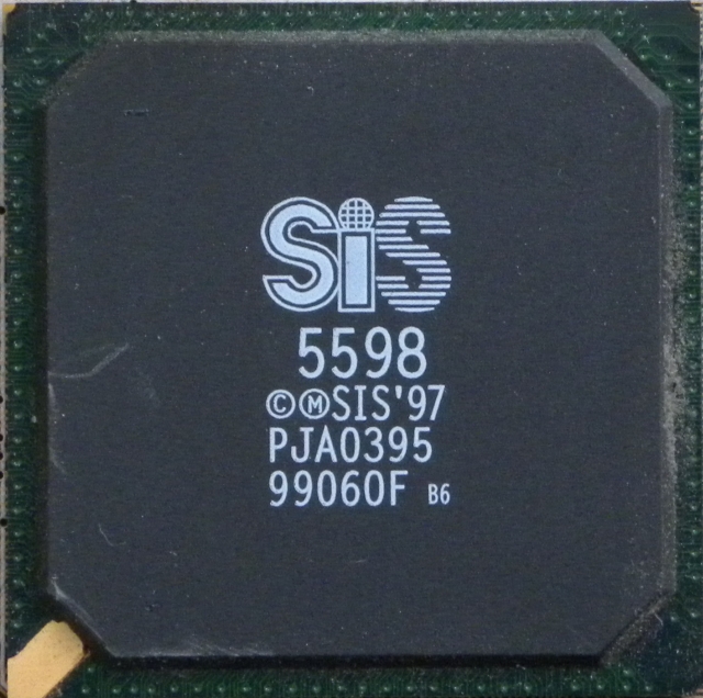 The market demanded for competitors to Intel's 430TX chipset, and until recently the only answer to those demands was VIA's VP2 chipset. However, Silicon Integrated Systems, commonly known as SiS, released a successor to their popular 5571 chipset, the SiS 5597 chipset and a variant of it, the SiS 5598. Those two single chip solutions are versatile enough to be used in virtually any form factor (LPX, NLX, AT, ATX) in a motherboard. Although very little is known about the 5597/98 series, some of the features of the chipset include:
-
onboard VGA
-
UltraDMA support
-
SDRAM support
-
ACPI support
| Common Name | SiS 5597/5598 | |
| Chipset Packaging | Number of chips | 1 |
| Packaging Type | 1 x 480-pin BGA | |
| CPU Support | Number of CPUs | 1 |
| AMD CPUs Supported | K5, K6 | |
| Cyrix CPUs Supported | 6x86 (M1), 6x86MX (M2) w/ Linear Burst Mode | |
| Intel CPUs Supported | Pentium, Pentium MMX | |
| Cache | Type | Synchronous Pipeline Burst Cache |
| Maximum Supported Size | 384MB | |
| Maximum Cacheable DRAM Area | 128MB | |
| Memory | Maximum DRAM Supported | 384MB |
| BEDO DRAM Read Timings (66MHz) | N/A | |
| EDO DRAM Read Timings (66MHz) | 5-2-2-2 | |
| FPM DRAM Read Timings (66MHz) | 5-3-3-3 | |
| SDRAM Read Timings (66MHz) | 5-1-1-1 | |
| Data Path to Memory | 64-bits | |
| ECC Support | No | |
| Hard Disk Controller | Chip | Integrated Controller |
| Busmastering Support | Yes | |
| UltraDMA Support | Yes | |
| Max. Theoretical Transfer Rate | PIO Mode 5/DMA Mode 3 (33.3MB/S) | |
| PCI Interface | Supported PCI Bus Speeds | 25, 30, 33 MHz |
| Concurrent PCI | Yes | |
| Async. PCI Bus Speed | Yes | |
| PCI Specification | 2.1 (66 MHz max.) | |
| Power Management | PC97 Compliance | Yes |
| Suspend to Disk | Yes | |
| HDD Power Down | Yes | |
| Modem Wakeup | Yes | |
| System Suspend | Yes | |
| Video | AGP Support | No |
| Unified Memory Architecture | Yes (onboard VGA) | |
| Peripheral Support | USB Support | Yes |
| Plug and Play Port | Yes | |
| Write Buffers | CPU-to-DRAM | Unknown |
| CPU-to-PCI | Unknown | |
| PCI-to-DRAM | Unknown | |
| Officially Supported Bus Speeds | 50, 60, 66, 75 MHz | |
| Unofficially Achieved Bus Speeds | 83 MHz | |
SiS 630 Chipset
This chipset is a single-chip, and is compatible with PC99 and PCI 2.2. It supports Pentium II, Pentium III and Celeron processors. It supports PC-133 SDRAM as well as VCRAM (?), and holds three dual inline memory modules (DIMMs) for a maximum of 1.5GB main memory. SiS630 also supports Ultra ATA 66 IDE and five "OpenHCI" USB ports. Something called ultra-AGP(TM) architecture is also mentioned as well as digital flat panel interfaces for LCD and TV output. Even 10/100M Fast Ethernet is included on-chip.
The 630 comprises the northbridge and an SiS 960 (southbridge I/O chip) as well as the real 128-bit 2D/3D graphics engine (SiS300) all into one single chip.
VIA Apollo Master (aka VT82C575M & VT82C577M) - 1995
Used on Socket 5 motherboards. Provided 66 MHz FSB and supported up to 1 GB of memory.
VIA VP1 Chipset (aka VT82C580VP Apollo 1) - 1996
 VIA's first attempt for the "gold" in the chipset market was with their 580VP chipset, commonly known as the VIA Apollo VP-1. Although when looked at now it seems like a poor design, during the time of the Intel 430FX chipset and the early days of the 430HX, the VP-1 was simply the best option for most users.
While Intel was boasting support for EDO and PIO Mode 4 hard drives, VIA stole the limelight with support for not only EDO, but BEDO and SDRAM as well as UltraDMA hard drives over a year before Intel ever thought about supporting such options. The performance of the VP-1 today still isn't up to par with solutions from Intel and even more recent VIA contributions, however if you are looking for a low cost, feature rich chipset solution the Apollo VP-1 is the answer to your prayers.
It was this very design that inspired the design of the ever so popular VIA VP2 chipset as well as the VPX chipset which followed the release of the successful VP-1. Unfortunately VIA's VP-1 doesn't boast some of the Power Saving features found in the PC97 compliant VPX/97 and VP2/97 chipsets which makes it a viable competitor for Intel's 430FX and possibly even VX chipsets, however not for Intel's TX chipset which clearly holds the advantage is this case.
Click here to download the VP1 data sheet.
| Common Name | Apollo VP-1 | |
| Chipset Packaging | Number of chips | 3 (VT82C585VP, VT82C586, VT82C587VP) |
| Packaging Type | 2 x 208-pin QFP; 1 x 100-pin QFP | |
| CPU Support | Number of CPUs | 1 |
| AMD CPUs Supported | K5, K6 | |
| Cyrix CPUs Supported | 6x86 (M1), 6x86MX (M2) w/ Linear Burst Mode | |
| Intel CPUs Supported | Pentium, Pentium MMX | |
| Cache | Type | Asynchronous/Synchronous Pipeline Burst Cache |
| Maximum Supported Size | 2048KB | |
| Maximum Cacheable DRAM Area | 512MB | |
| Memory | Maximum DRAM Supported | 512MB |
| BEDO DRAM Read Timings (66MHz) | 5-1-1-1 | |
| EDO DRAM Read Timings (66MHz) | 5-2-2-2 | |
| FPM DRAM Read Timings (66MHz) | 5-3-3-3 | |
| SDRAM Read Timings (66MHz) | 5-1-1-1 | |
| Data Path to Memory | 64-bits | |
| ECC Support | No | |
| Hard Disk Controller | Chip | VIA BMIDE Controller (VT82C586) |
| Busmastering Support | Yes | |
| UltraDMA Support | Yes | |
| Max. Theoretical Transfer Rate | PIO Mode 5/DMA Mode 3 (33.3MB/S) | |
| PCI Interface | Supported PCI Bus Speeds | 25, 30, 33 MHz |
| Concurrent PCI | No | |
| Async. PCI Bus Speed | No | |
| PCI Specification | 2.0 (66 MHz max.) | |
| Power Management | PC97 Compliance | No |
| Suspend to Disk | No | |
| HDD Power Down | Yes | |
| Modem Wakeup | No | |
| System Suspend | No | |
| Video | AGP Support | No |
| Unified Memory Architecture | Yes | |
| Peripheral Support | USB Support | Yes |
| Plug and Play Port | Yes | |
| Write Buffers | CPU-to-DRAM | 16 QWords (?) |
| CPU-to-PCI | 6 DWords (?) | |
| PCI-to-DRAM | 48 DWords (?) | |
| Officially Supported Bus Speeds | 50, 60, 66 MHz | |
| Unofficially Achieved Bus Speeds | 75 MHz | |
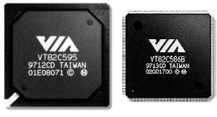
VIA VP2 Chipset (aka VT82C590 Apollo VP2/97) - 1997
 With the success VIA attained with the VP-1 and VPX chipsets it was time to drop a huge bomb on the competition by announcing a head to head competitor of Intel's latest and greatest 430TX chipset. VIA did just that with the announcement of the VP2/97 chipset, and it was that announcement that allowed them to gain the support of some of the industry's biggest names, including Advanced Micro Devices with the release of their AMD K6 Microprocessor.
The VIA VP2/97 chipset combines the best features found in all Socket-7 chipsets, from BEDO and SDRAM support to UMA and UltraDMA support, the VP2/97 topples the competition with a rich feature set. The unique two chip solution from VIA packs a strong punch with, once again, a maximum of 512MB (all cached) RAM complimented by the large 2MB of L2 cache possible with the VP2/97. Supporting all processor classes from the early Pentium Classic to the Cyrix 6x86MX with support for Intel and Linear Burst Mode SRAM transfers the VP2/97 is truly a chipset for the masses.
Like Intel's TX chipset, the power saving features on the VP2/97 are tremendous which is a direct result of its PC97 compliance. The VP2/97 is in a class of its own since NO other Socket-7 chipset can even begin to support the features the VP2/97 boasts. The only downside to the VP2/97 is that it doesn't support AGP, which will be featured in the successor to the VP2/97, the VIA VP3 chipset.
AMD licensed the VIA Apollo VP2/97 core logic architecture as its AMD 640 chipset.
Click here to download the VP2 data sheet.
| Common Name | Apollo VP2/97 | |
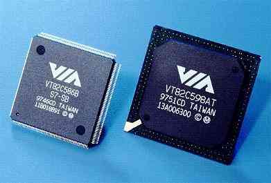
| Chipset Packaging | Number of chips | 2 (VT82C595 Northbridge, VT82C586B Southbridge) |
| Packaging Type | 1 x 328-pin BGA; 1 x 208-pin QFP | |
| CPU Support | Number of CPUs | 1 |
| AMD CPUs Supported | K5, K6 | |
| Cyrix CPUs Supported | 6x86 (M1), 6x86MX (M2) w/ Linear Burst Mode | |
| Intel CPUs Supported | Pentium, Pentium MMX | |
| Cache | Type | Synchronous Pipeline Burst Cache |
| Maximum Supported Size | 2048KB | |
| Maximum Cacheable DRAM Area | 512MB | |
| Memory | Maximum DRAM Supported | 512MB |
| BEDO DRAM Read Timings (66MHz) | 5-1-1-1 | |
| EDO DRAM Read Timings (66MHz) | 5-2-2-2 | |
| FPM DRAM Read Timings (66MHz) | 5-3-3-3 | |
| SDRAM Read Timings (66MHz) | 3-1-1-1 | |
| Data Path to Memory | 64-bits | |
| ECC Support | Yes | |
| Hard Disk Controller | Chip | VIA South Bridge Controller (VT82C586B) |
| Busmastering Support | Yes | |
| UltraDMA Support | Yes | |
| Max. Theoretical Transfer Rate | PIO Mode 5/DMA Mode 3 (33.3MB/S) | |
| PCI Interface | Supported PCI Bus Speeds | 25, 30, 33 MHz |
| Concurrent PCI | Yes | |
| Async. PCI Bus Speed | No | |
| PCI Specification | 2.0 (66 MHz max.) | |
| Power Management | PC97 Compliance | Yes |
| Suspend to Disk | Yes | |
| HDD Power Down | Yes | |
| Modem Wakeup | Yes | |
| System Suspend | Yes | |
| Video | AGP Support | No |
| Unified Memory Architecture | Yes | |
| Peripheral Support | USB Support | Yes |
| Plug and Play Port | Yes | |
| Write Buffers | CPU-to-DRAM | 16 QWords |
| CPU-to-PCI | 6 DWords | |
| PCI-to-DRAM | 48 DWords | |
| Officially Supported Bus Speeds | 50, 60, 66 MHz | |
| Unofficially Achieved Bus Speeds | 68, 75, 83.3 MHz | |
Example VIA Apollo VP-2/97 chipset motherboards:
FIC PT-2007 |
FIC PA-2011 |


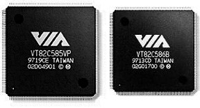
VIA VPX Chipset (aka Apollo VPX/97) - 1997
 VIA is now the ultimate competitor to Intel's tyranny in the Chipset market, and although they aren't as large or as powerful as the microprocessor giant they produce chipsets that have toppled even Intel's best efforts in this industry.
With the success of the original Apollo VP chipset, a supposed competitor of the Intel 430FX chipset although it blew it away in most instances, VIA decided to implement some next generation features into their hot topic VPX chipset. By raising the cacheable memory limit to 512MB, giving the user a maximum of 2MB of L2 cache, and allowing us to take advantage of such features as UltraDMA hard drives and SDRAM (features only found in Intel's TX and LX chipsets) VIA accomplished in producing a superior product in nearly every aspect to Intel's lackluster 430 series of chipsets. VIA embraced all CPU manufacturers with the release of the Apollo VPX by allowing support for normal Intel Burst Modes as well as the elusive Linear Burst Mode reserved for IBM/Cyrix processors.
Unfortunately many motherboard manufacturers couldn't properly harness this power, and therefore quite a few users were disappointed with VPX based systems since they were poorly designed. However, a few companies were able to take advantage of the amazing capabilities of this chipset. Among these companies, FIC, seemed to be the most successful in achieving the maximum potential of the VPX chipset with their PA-2010+.
The VPX chipset features many of the useful options we all loved from the HX and VX chipsets, while adding some of its own unique characteristics such as BEDO DRAM support with a timing of 5-1-1-1. The VPX, like Intel's VX chipset supports UMA and SDRAM, however the VPX's SDRAM timings are much faster than those of Intel's VX chipset. If you combine the extensive memory support of the VPX chipset, as well as its support for UltraDMA/33 hard drives the VPX begins to look much less like a competitor and much more like a dominator in the chipset industry.
The VPX chipset is also fully PC97 compliant, however a more affordable version without PC97 compliance is available for entry level systems consisting of the VT82C585VPX and VT82C586A instead of the VT82C585VPX northbridge and VT82C586B southbridge controllers.
Click here to download the VPX data sheet.
| Common Name | Apollo VPX/97 | |
| Chipset Packaging | Number of chips | 2 (VT82C595 Northbridge Controller, VT82C586B Southbridge) |
| Packaging Type | 2 x 208-pin QFP | |
| CPU Support | Number of CPUs | 1 |
| AMD CPUs Supported | K5, K6 | |
| Cyrix CPUs Supported | 6x86 (M1), 6x86MX (M2) w/ Linear Burst Mode | |
| Intel CPUs Supported | Pentium, Pentium MMX | |
| Cache | Type | Asynchronous/Synchronous Pipeline Burst Cache |
| Maximum Supported Size | 2048KB | |
| Maximum Cacheable DRAM Area | 512MB | |
| Memory | Maximum DRAM Supported | 512MB |
| BEDO DRAM Read Timings (66MHz) | 5-1-1-1 | |
| EDO DRAM Read Timings (66MHz) | 5-2-2-2 | |
| FPM DRAM Read Timings (66MHz) | 5-3-3-3 | |
| SDRAM Read Timings (66MHz) | 3-1-1-1 | |
| Data Path to Memory | 64-bits | |
| ECC Support | No | |
| Hard Disk Controller | Chip | VIA South Bridge Controller (VT82C586B) |
| Busmastering Support | Yes | |
| UltraDMA Support | Yes | |
| Max. Theoretical Transfer Rate | PIO Mode 5/DMA Mode 3 (33.3MB/S) | |
| PCI Interface | Supported PCI Bus Speeds | 25, 30, 33 MHz |
| Concurrent PCI | Yes | |
| Async. PCI Bus Speed | Yes | |
| PCI Specification | 2.0 (66 MHz max.) | |
| Power Management | PC97 Compliance | Yes |
| Suspend to Disk | Yes | |
| HDD Power Down | Yes | |
| Modem Wakeup | Yes | |
| System Suspend | Yes | |
| Video | AGP Support | No |
| Unified Memory Architecture | Yes | |
| Peripheral Support | USB Support | Yes |
| Plug and Play Port | Yes | |
| Write Buffers | CPU-to-DRAM | 16 QWords |
| CPU-to-PCI | 6 DWords | |
| PCI-to-DRAM | 48 DWords | |
| Officially Supported Bus Speeds | 50, 60, 66, 75 MHz | |
| Unofficially Achieved Bus Speeds | 68, 83.3 MHz | |
Example VIA Apollo VPX/97 chipset motherboards:
FIC PA-2010+ |

VIA VP3 Chipset (aka VT82C Apollo VP3) - 1997
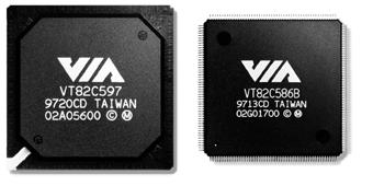 Hoping to destroy the competition Intel announced and released their 440LX chipset late in 1997 with support for AGP, however that AGP support is limited to the Slot-1 Architecture of the Pentium II since Intel announced that they would not produce an AGP-equipped Pentium Chipset. This produced a tremendous opportunity for some of the other chipset manufacturers to step up and satisfy the market. VIA, being the leading contender for Intel's throne, decided to use this to their advantage. The result of their efforts? The VIA Apollo VP3 Chipset, the first AGP-capable Pentium Chipset.
Here's what they said at the time: "Take all of the features of the VP2/97 chipset, double the CPU-to-DRAM Write Buffers, add a full gigabyte of cacheable memory area (which is greater than the 512MB supported by the Pentium II !!!) and AGP support and you get the Apollo VP3 chipset. As the VP2/97 was essentially a combination of the Intel HX and TX chipsets, the VP3 is a combination of the VIA VP2 and the Intel 440LX chipsets. Although the performance of the VP3 has yet to be proven, it will soon by FIC with the release of their PA-2012, the very first Socket-7 AGP Motherboard. VIA has a huge hit on their hands with the combination of the success of the VP2/97 and the imminent success of the VP3 chipset.
Unfortunately there are two significant "let downs" the VP3 chipset leaves us with. The first isn't all that prominent, just that the VP3 doesn't support BEDO DRAM like its predecessors the VP2 and VPX did. Its support for SDRAM as well as DDR-SDRAM does compensate for that shortcoming so it really isn't a huge problem for most users. The big letdown is the lack of a 100MHz bus speed support natively with the VP3 chipset, we will unfortunately have to wait for the next stop in VIA's travels for 100MHz bus speed support with the MVP3 (Mobile VP3)."
Click here to download the VP3 data sheet.
| Common Name | Apollo VP3 | |
| Chipset Packaging | Number of chips | 2 (VT82C597 System Controller, VT82C586B PCI-to-ISA Bridge) |
| Packaging Type | 1 x 472-pin BGA; 1 x 208-pin QFP | |
| CPU Support | Number of CPUs | 1 |
| AMD CPUs Supported | K5, K6 | |
| Cyrix CPUs Supported | 6x86 (M1), 6x86MX (M2) w/ Linear Burst Mode | |
| Intel CPUs Supported | Pentium, Pentium MMX | |
| Cache | Type | Synchronous Pipeline Burst Cache |
| Maximum Supported Size | 2048KB | |
| Maximum Cacheable DRAM Area | 1GB | |
| Memory | Maximum DRAM Supported | 1GB |
| BEDO DRAM Read Timings (66MHz) | N/A | |
| EDO DRAM Read Timings (66MHz) | 5-2-2-2 | |
| FPM DRAM Read Timings (66MHz) | 5-3-3-3 | |
| SDRAM Read Timings (66MHz) | 3-1-1-1 | |
| Data Path to Memory | 64-bits | |
| ECC Support | Yes | |
| Hard Disk Controller | Chip | VIA BMIDE Controller (VT82C586B) |
| Busmastering Support | Yes | |
| UltraDMA Support | Yes | |
| Max. Theoretical Transfer Rate | PIO Mode 5/DMA Mode 3 (33.3MB/S) | |
| PCI Interface | Supported PCI Bus Speeds | 25, 30, 33 MHz |
| Concurrent PCI | Yes | |
| Async. PCI Bus Speed | No | |
| PCI Specification | 2.0 (66 MHz max.) | |
| Power Management | PC97 Compliance | Yes |
| Suspend to Disk | Yes | |
| HDD Power Down | Yes | |
| Modem Wakeup | Yes | |
| System Suspend | Yes | |
| Video | AGP Support | Yes |
| Unified Memory Architecture | No | |
| Peripheral Support | USB Support | Yes |
| Plug and Play Port | Yes | |
| Write Buffers | CPU-to-DRAM | 32 QWords |
| CPU-to-PCI | 6 DWords | |
| PCI-to-DRAM | 48 DWords | |
| Officially Supported Bus Speeds | 50, 60, 66 MHz | |
| Unofficially Achieved Bus Speeds | Unknown | |
VIA MVP3 Chipset (aka VT82C Apollo Mobile VP3) - 1998
 With ALi boasting support for the 100MHz Frontside Bus in their new Aladdin V chipset and with a large cacheable memory area, how could VIA resist but to release a Super7 candidate of their own? Originally, the VIA VP3 was expected to be the very first 100MHz + Socket 7 + AGP motherboard, but unfortunately VIA dropped a bombshell on the market by announcing that the VP3 wouldn't support any bus speeds greater than 66MHz. At the same time VIA hinted at a Mobile-VP3 chipset, the MVP3, that would support the 100MHz bus speed & AGP. Under a year later the MVP3 chipset was almost ready to make its grand-entrance, but how grand would it be?
In spite of the name, the Mobile VP3 can be used in both Desktop and Mobile motherboard solutions, this versatility would prove to be beneficial for VIA since no other chipset manufacturer has a chipset that will officially run the 100MHz on a Notebook system. In the desktop arena, the MVP3 became a competitor to the Aladdin V by ALi, with both chipsets supporting all of the features the Intel TX chipset did adding support for a 100MHz Frontside bus, as well as AGP 2x support. The MVP3 differed from the Aladdin V in two major areas, both involving RAM...let's explore the two differences.
While the Aladdin V only supports EDO, FPM, and SDRAM, the MVP3 supports JEDEC BDDR SDRAM-II (Bi Directional Double Data Rate SDRAM), Virtual Channel SDRAM, and Enhanced SDRAM. While those last few SDRAM types are next to impossible to come across that may change if the demand for SDRAM-II modules increases, possibly by the success of a chipset that supports the standard. Its a heavy weight to put on the MVP3's unreleased shoulders, but it is there nevertheless.
Speaking of RAM, the MVP3 chipset introduces a unique feature into the Super7 arena, the ability to run the Memory Bus Speed at 66MHz, while using a 100MHz Bus Speed to derive the Processor Clock. This means that, in theory, you could even re-use your old generic 60ns EDO SIMMs on a MVP3 motherboard. Not a bad feature for VIA to include.
The only other real difference between the MVP3 and the Aladdin V is that the MVP3 doesn't feature any Internal L2 cache bits/Tag RAM bits, making high quality L2 cache with a fast Tag RAM chip a necessity for all MVP3 boards if you plan on using them with the 100MHz bus speed. This introduces a new factor into achieving system stability, L2 cache quality, if a manufacturer of a MVP3 motherboard decides to skimp on the L2 cache and include 8 or even 10ns SRAM chips, expect to have problems galore at 100MHz.
An interesting note, unlike all previous VIA Socket-7 chipsets, the MVP3 only features an integrated 8-bit Tag comparator while the VP2 for example features an integrated 10-bit Tag comparator. Translation? Don't expect MVP3 motherboards to be able to cache the supported 1GB of RAM, in combination with the L2 cache sizes and Tag RAM chips that will be used on most MVP3 motherboards, expect cacheable memory areas to range from 256MB down to 64MB. While waiting for an official word from VIA on this issue, it seems highly unlikely that MVP3 motherboards will be able to compete with Aladdin V boards in terms of cacheable memory areas.
Performance wise, in spite of the fewer CPU-to-DRAM write buffers, the MVP3 should be on the heels of the Aladdin V, outperforming the Intel TX chipset at the 66MHz bus speed and leaving it behind when clocked at 100MHz.
VIA has been in the lime light of the chipset industry for much longer than Acer Labs has, so it'll take quite a bit for VIA to throw in the towel in the Super7 battle. Expect the MVP3 to be the Aladdin V's biggest competitor, in the end it will most likely come down to a battle among motherboard manufacturers to completely harness the immense power of one of these two chipsets.
The VIA Apollo MVP3 was loved by over-clockers for its ability to desynchronise the FSB from the PCI/ISA/AGP bus but had slightly less good AGP performance.
Apparently there have been reports that the MVP3 doesn't play nicely with nVidia graphics cards.
Click here to download the MVP3 data sheet.
| Common Name | Apollo MVP3 | |
| Chipset Packaging | Number of chips | 2 (VT82C598AT System Controller, VT82C586B PCI-to-ISA Bridge) |
| Packaging Type | 1 x 476-pin BGA; 1 x 208-pin QFP | |
| CPU Support | Number of CPUs | 1 |
| AMD CPUs Supported | K5, K6, K6-3D | |
| Cyrix CPUs Supported | 6x86 (M1), 6x86MX (M2) w/ Linear Burst Mode | |
| Intel CPUs Supported | Pentium, Pentium MMX | |
| Cache | Type | Synchronous Pipeline Burst Cache |
| Maximum Supported Size | 2048KB | |
| Maximum Cacheable DRAM Area | ??? | |
| Memory | Maximum DRAM Supported | 1GB |
| BEDO DRAM Read Timings (66MHz) | N/A | |
| EDO DRAM Read Timings (66MHz) | 5-2-2-2 | |
| FPM DRAM Read Timings (66MHz) | 5-3-3-3 | |
| SDRAM Read Timings (66MHz) | 3-1-1-1 | |
| Data Path to Memory | 64-bits | |
| ECC Support | Yes | |
| Hard Disk Controller | Chip | VIA BMIDE Controller (VT82C586B) |
| Busmastering Support | Yes | |
| UltraDMA Support | Yes | |
| Max. Theoretical Transfer Rate | PIO Mode 5/DMA Mode 3 (33.3MB/S) | |
| PCI Interface | Supported PCI Bus Speeds | 25, 30, 33 MHz |
| Concurrent PCI | Yes | |
| Async. PCI Bus Speed | Yes (Pseudo Synchronous) | |
| PCI Specification | 2.1 (66 MHz max.) | |
| Power Management | PC97 Compliance | Yes |
| Suspend to Disk | Yes | |
| HDD Power Down | Yes | |
| Modem Wakeup | Yes | |
| System Suspend | Yes | |
| Video | AGP Support | Yes |
| Unified Memory Architecture | No | |
| Peripheral Support | USB Support | Yes |
| Plug and Play Port | Yes | |
| Write Buffers | CPU-to-DRAM | 16 QWords |
| CPU-to-PCI | 5 DWords | |
| PCI-to-DRAM | 48 DWords | |
| Officially Supported Bus Speeds | 50, 60, 66, 75, 83, 100 MHz | |
| Unofficially Achieved Bus Speeds | Unknown | |
Example VIA Apollo MVP3 chipset motherboards:
EPOX EP-MVP3G2 |
DFI K6XV3+/66 |
VIA MVP4 Chipset - 1998
 This chipset introduced an integrated graphics controller and new ATA-66 interface for improved hard disk performance.
The chipset consisted of the VT82C501 North Bridge, and the VT82C686 'Super South Bridge'.
This southbridge included integrated AC'97 2.0 audio, ACPI, USB, and advanced mobile PC power management.
VIA Apollo Pro Chipset - 1998
While Intel accepted the fact that they had the sole production of Slot-1 chipset solutions in their hands, VIA was working hard, both on the legal and engineering ends of things, to produce the perfect Slot-1 compatible chipset they could possibly produce, the results? The VIA Apollo Pro chipset.
Supporting all of the features of the Intel 440BX AGPSet, the Apollo Pro is much more than an alternative to the BX Chipset as it brings much more than AGP and SDRAM support to the game. Support for 5 PCI master devices (compared to the 3 PCI masters on Intel chipsets) make the Apollo Pro ideal for an ISA Slot-less motherboard, in theory, with the use of an additional PCI-to-PCI bridge, a motherboard featuring 7 PCI slots could be constructed although only 6 of them would be usable at one time as long as a card populated the AGP slot. Expect to see a minimum of 5 PCI slots on most Apollo Pro based motherboard solutions. In addition to that, the Apollo Pro, like the VIA MVP3, does support the operation of the memory bus at an external frequency identical to that of the AGP Clock. Meaning you can run your memory banks at the 66MHz Front Side Bus, while your processor's speed is derived from the 100MHz FSB. This will allow you to re-use your old PC66 DIMMs and even your old EDO/FP DIMMs so long as they work at the 66MHz FSB.
The Apollo Pro's supported DRAM types extends far beyond the normal EDO/FP/SDRAM list, to include DDR (Double Data Rate) SDRAM. While this looks wonderful on paper, the absence of DDR SDRAM in the mainstream market will keep that feature from becoming a reason to opt for an Apollo Pro based board over an Intel chipset based model. Expect performance of Apollo Pro-based Pentium II boards to be at least on par with that of well designed BX motherboards, with the first boards shipping in the next month or two we should soon be able to find out if the Apollo Pro is everything it is cracked up to be.
A downside to the Apollo Pro is that, unlike the Intel LX/BX/GX series, you must use VIA's own AGP GART drivers to get the full benefit of the supported AGP port which may introduce some issues with future video cards and chipsets, nothing that a simple driver patch won't fix but something to keep in mind.
Click here to download the Apollo Pro data sheet.
| Common Name | VIA Apollo Pro Chipset | |
| Chipset Packaging | Number of chips | 1 (VT82C691 Northbridge) |
| Packaging Type | 1 x 492-pin BGA | |
| CPU Support | Number of CPUs | 1 |
| AMD CPUs Supported | N/A | |
| Cyrix CPUs Supported | N/A | |
| Intel CPUs Supported | Pentium II, Pentium Pro | |
| Cache | Type | N/A on chip |
| Maximum Supported Size | N/A on chip | |
| Maximum Cacheable DRAM Area | N/A on chip | |
| Memory | Maximum DRAM Supported | 1GB |
| BEDO DRAM Read Timings (100MHz) | N/A | |
| EDO DRAM Read Timings (100MHz) | X-2-2-2 | |
| FPM DRAM Read Timings (100MHz) | X-4-4-4 | |
| SDRAM Read Timings (100MHz) | X-1-1-1 | |
| Data Path to Memory | 64-bits | |
| ECC Support | Yes | |
| Hard Disk Controller | Chip | VT82C596 South Bridge |
| Bus Mastering Support | Yes | |
| UltraDMA Support | Yes | |
| Max. Theoretical Transfer Rate | PIO Mode 5/DMA Mode 3 (33.3MB/S) | |
| PCI Interface | Supported PCI Bus Speeds | 30, 33 MHz |
| Async. PCI Bus Speed | No | |
| PCI Specification | 2.1 (66 MHz max.) | |
| Power Management | PC97 Compliance | Yes |
| Suspend to Disk | Yes | |
| HDD Power Down | Yes | |
| Modem Wakeup | Yes | |
| System Suspend | Yes | |
| Video | AGP Support | Yes (66/133) |
| Unified Memory Architecture | No | |
| Peripheral Support | USB Support | Yes |
| Plug and Play Port | Yes | |
| Officially Supported Bus Speeds | 66, 100 MHz | |
| Unofficially Achieved Bus Speeds | 112, 124MHz | |
VIA VXPro / VXPro+ Chipset
Here is an odd chipset you might've heard of in your experiences with motherboards and chipsets, the elusive VXPro chipset, found mostly in PCChips motherboards. Although it is often referred to as a cheap imitation of the Intel 430VX chipset, the VXPro does have its advantages over Intel's design, mainly dealing with cost.
The VXPro+ Chipset fully supports UltraDMA hard drives and SDRAM, unfortunately it doesn't feature the fast SDRAM timings found in the Intel TX and VIA Apollo VP2 chipsets which degrade its quality as a whole. However, the VXPro was never intended to be marketed under any labels, although the technology was apparently licensed to PCChips for use in their motherboards by VIA. VXPro chipset would appear to be loosely based on the VIA Apollo VP-1, however it seems to be a much cheaper version of it directed at entry level users. The VXPro was intended to be more of a head to head competitor of Intel's VX chipset, including features such as UMA support.
As far as most information sources goes, the VXPro chipset still limits the cacheable memory area to 64MB and unfortunately it doesn't support the maximum 2MB of L2 cache found in the superior Apollo VP-1. The VXPro chipset does however support the use of Concurrent PCI/CPU operations as well as an asynchronous PCI bus (i.e. the PCI bus can be set to 33MHz regardless of the external bus speed). The only area in which the VXPro really excels however, aside from the fact that the VXPro+ supports the UltraATA extension, is its amazing price. A motherboard built around the VXPro chipset will most likely go for about $60 which isn't bad for someone looking for an affordable solution for a second or third computer, possibly even a low cost business workstation.
| Common Name | VXPro | |
| Chipset Packaging | Number of chips | 2 (VT82C585, VT82C586) |
| Packaging Type | 2 x 208-pin QFP | |
| CPU Support | Number of CPUs | 1 |
| AMD CPUs Supported | K5, K6 | |
| Cyrix CPUs Supported | 6x86 (M1), 6x86MX (M2) | |
| Intel CPUs Supported | Pentium, Pentium MMX | |
| Cache | Type | Asynchronous/Synchronous Pipeline Burst Cache |
| Maximum Supported Size | 512KB | |
| Maximum Cacheable DRAM Area | 64MB | |
| Memory | Maximum DRAM Supported | 128MB |
| BEDO DRAM Read Timings (66MHz) | N/A | |
| EDO DRAM Read Timings (66MHz) | 5-2-2-2 | |
| FPM DRAM Read Timings (66MHz) | 5-3-3-3 | |
| SDRAM Read Timings (66MHz) | 7-1-1-1 | |
| Data Path to Memory | 64-bits | |
| ECC Support | No | |
| Hard Disk Controller | Chip | VIA BMIDE Controller (VT82C586) |
| Busmastering Support | Yes | |
| UltraDMA Support | Yes | |
| Max. Theoretical Transfer Rate | PIO Mode 5/DMA Mode 3 (33.3MB/S) | |
| PCI Interface | Supported PCI Bus Speeds | 25, 30, 33 MHz |
| Concurrent PCI | Yes | |
| Async. PCI Bus Speed | Yes | |
| PCI Specification | 2.0 (66 MHz max.) | |
| Power Management | PC97 Compliance | No |
| Suspend to Disk | No | |
| HDD Power Down | Yes | |
| Modem Wakeup | No | |
| System Suspend | No | |
| Video | AGP Support | No |
| Unified Memory Architecture | Yes | |
| Peripheral Support | USB Support | Yes |
| Plug and Play Port | Yes | |
| Write Buffers | CPU-to-DRAM | Unknown |
| CPU-to-PCI | Unknown | |
| PCI-to-DRAM | Unknown | |
| Officially Supported Bus Speeds | 50, 60, 66 MHz | |
| Unofficially Achieved Bus Speeds | 75, 83 MHz | |