PC Chips M590 Motherboard - Part 3
26th April 2023
In Part 2 we got the PC Chips M590 powered up and ran some basic synthetic tests using an AMD K6-2 533 and older 72-pin SIMM memory. In this Part 3 I will conduct some tests using DIMM memory for comparison.
The DIMMs
I have about 18 sticks of DIMM memory to choose from in the collection. Most of them are PC100 and a few are PC133. The M590 only supports up to PC100 memory, so I have chosen two of these:
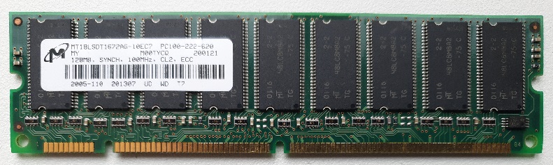

The DIMMs (128 MB PC100 ECC CL2)
The BIOS provides an option of either 10ns or 12ns SDRAM memory. I will keep it at 12ns for my initial tests. Oh, and I've kept the CPU settings as per the last test, so it's firing on all cylinders at about 540 MHz (90 MHz FSB and 6x multiplier).
Here's SpeedSys and CacheChk:
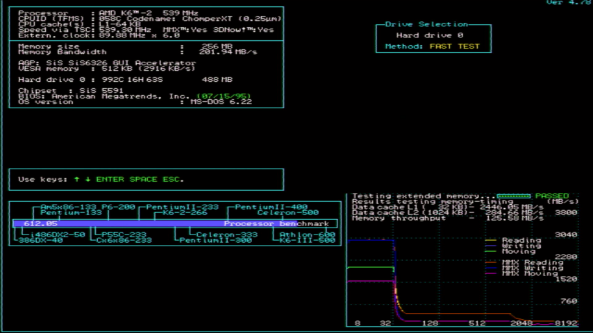
Hmmm, well that's disappointing. The memory throughput according to SpeedSys reached 125.58 MB/s with the DIMMs, compared with 89.13 MB/s on the SIMMs - a 41% increase. CacheChk, which incorrectly reports only 64 MB and not the full 256 MB saw a 36% increase in memory bandwidth over the SIMMs. Let's tweak the memory settings in the BIOS to see if we can get more improvement...
There are a good number of settings we can change here:
- SDRAM Speed (either 10ns or 12ns) - changed to 10ns
- Refresh Queue Depth (0, 4, 8 or 12) - often called Refresh Cycle Time - if your memory chips can support it, lowering the number of cycles will reduce the latency, i.e. improve performance, but possibly increase temperature. I changed this to 0ns.
- SDRAM CAS latency (2T or 3T) - changed from 3T to 2T, as my DIMM modules are "CL2"-rated.

Re-running SpeedSys with these faster BIOS memory settings has increased the memory bandwidth from 202 MB/s to 218 MB/s, and memory throughput is now 132.53 MB/s. An 8% improvement - not amazing. CacheChk also reports about an 8% improvement.
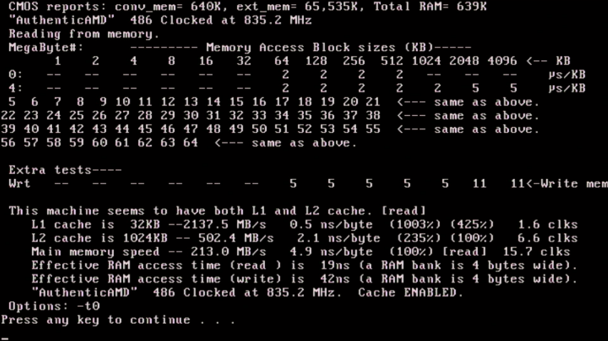
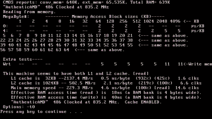
Going back into the BIOS and choosing "Manual" DRAM configuration allows us to choose the RAS SDRAM timing, RAS precharge time and SDRAM read timing manually. I've now set them to be 5T/4T, 2T, and 51111111 respectively, keeping the previous faster settings in place also:

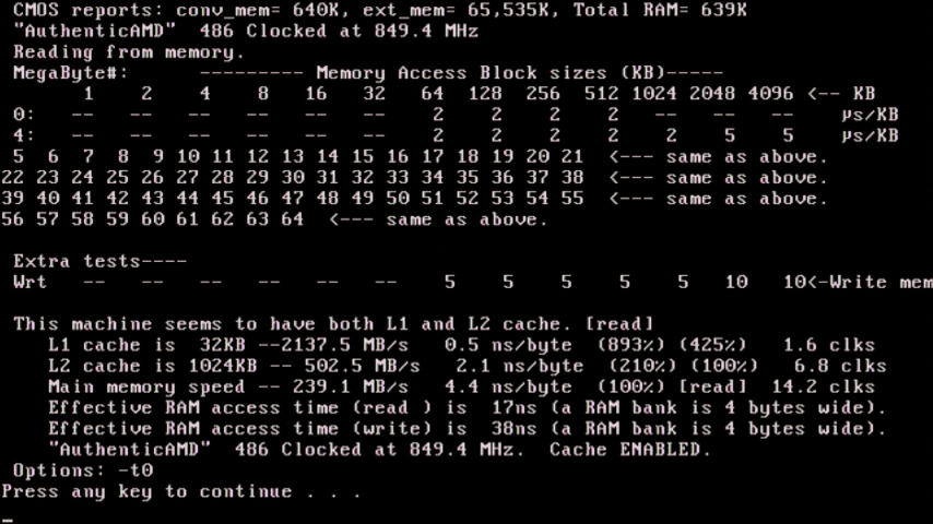
OK, that's a bit more like it. SpeedSys now reports memory bandwidth of 227.78 MB/s - a 160% increase over the SIMMs (so 2.6x that of the SIMMs). The memory throughput is 140.3 MB/s which is a 57% increase over the SIMMs operating at their fastest. CacheChk's results show a similar increase of 52% over the SIMMs.
I ran the GoldMemory utility on this configuration too, and it benchmarked at 137 MB/s.
Knowing that we're only running these at 90 MHz instead of the full 100 MHz speed that PC100 is capable of means we'll never be really getting the most out of them. PC100 SDRAM takes one clock cycle to transfer 1 word of data, compared to EDO which takes two or three clock cycles to transfer the same, so the throughput I'd like to see is 2-3 times that of the SIMMs. It has a theoretical maximum data transfer rate of (clock x number of bits) / 8, so in the case of a PC100 DIMM, that's (100 x 64) / 8 = 800 MB/sec. For the PC Chips M590, we're only running a FSB of 89.88, so we would peak at 719 MB/sec.
So whilst running SDRAMs over SIMMs is absolutely giving us a decent performance bump, we're still way off that theoretical maximum. To understand this, it's worthwhile providing an understanding of SDRAM memory timings. You may see a DIMM having a set of numbers like '5-2-2-2' or '7-3-2-2'. What does these mean? Each number is the amount of time (latency) it takes for the chip to perform a specific task:
In order they are CL-tRCD-tRP-tRAS-CMD, with the following meanings:
- CL (CAS Latency) - The time it takes between a command having been sent to the memory and when it begins to reply to it. It is the time it takes between the processor asking for some data from the memory and then returning it.
- tRCD (RAS to CAS Delay) - The time it takes between the activation of the line (RAS) and the column (CAS) where the data are stored in the matrix.
- tRP (RAS Precharge) - The time it takes between disabling the access to a line of data and the beginning of the access to another line of data.
- tRAS (Active to Precharge Delay) - How long the memory has to wait until the next access to the memory can be initiated.
- CMD (Command Rate) - The time it takes between the memory chip having been activated and when the first command may be sent to the memory. Sometimes this value is not announced. It usually is T1 (1 clock cycle) or T2 (2 clock cycles).
Summary of EDO vs SDRAM
So with this very limited set of tests, I managed to see an increase in memory bandwidth of 160% (2.6 times better) - not as great as I would have hoped, but certainly shows it's well worth using DIMMs on a motherboard like this. Let me know what you would expect or have seen when comparing the performance of 72-pin EDO SIMMs against 168-pin SDRAM DIMMs.
Other CPUs
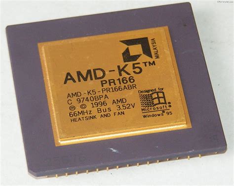 I attempted to use several AMD K5 CPUs in the M590, but it always failed to POST - nothing on-screen at all, and the POST card stopped on "06".
This is somewhat surprising for three reasons: Firstly, the Socket 7 standard is fully backward-compatible with the Socket 5 that the K5 would have been at home on. Secondly, PC Chips provided good support for the K5 on slightly earlier motherboards, and thirdly, the SiS5581 chipset is known to support both the K5 and K6.
I put this down to the BIOS code itself not including support for it, so it could be added with an unofficial BIOS update. I assume that because the K5 had been around for 2 years already, they simply didn't bother. Many other Super Socket 7 motherboard BIOSs do cater for the AMD K5, including other PC Chips motherboards such as the M570, M571, M573, M575 and M921.
More to come soon.... in Part 4 I will play some games using the onboard CMI8330 audio.