OPTi-based 386/486 Hybrid Motherboard - Part 1
27th March 2021
This week, I picked up a 386/486 hybrid motherboard from EBay. I've been looking for a late 386 board with VESA Local Bus for a while to do some testing on. The board is a Data Expert EXP3406 revision 1.1. According to the user manual its other name is OPTI-496XLC 3/486WB Cache Main Board - catchy, I know.

Despite what appears to be a very upgradeable motherboard, this would have been sold as a budget board in 1993, aimed at those who couldn't afford a 486DX. Premium motherboards at the time would possibly have had the then-new 72-pin SIMM sockets which were 32-bit, and possibly even PCI slots though these didn't really hit the consumer market until the year after.
Quick Visual Inspection
Looking around the board it appears to comprise the following:
- A soldered-in AMD Am386DX-40 CPU.
- OPTi 82C495XLC chipset.
- A socket for a math co-processor.
- Through-hole pins to support a 132-pin socket for an upgrade CPU.
- BIOS in a Winbond chip, and an AMI keyboard controller.
- Eight 30-pin SIMM slots.
- Two banks of L2 cache slots, one populated.
- Seven 16-bit ISA expansion slots of which 2 are Local Bus.
- AT P8/P9 power connector
- Full-size DIN keyboard socket
The previous owner had told me the board was working but had been repaired. The CMOS backup battery had leaked so he removed it.
Date-wise, the most recent date stamp on the motherboards' chips is week 31 of 1994, which is the big OPTi chip. So this board was manufactured after 1st August 1994 - very late for a 386-based board.
The Component Parts
The CPU
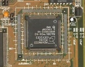 It is evident from looking around the CPU that the Data Expert EXP3406 was manufactured for both the 80386 and 80486 markets. It can support a 132-pin 80386 PQFP (Plastic Quad Flat Package) CPU or a 168-pin i486SX PQFP CPU - soldered-in. Either of these chips would have been pretty cheap to buy when this board first came out around 1993.
The Am386DX-40 as I have on this one was especially cost-effective and coincidentally was the fastest native 386 CPU ever produced. Launched in 1991 after some delays, AMD's Am386 was in a market that had already seen 2 years of Intel's dominance at the high end with their 80486DX, and the 80486SX was just being launched, aimed at the budget market. I would imagine this 386-based board would have been sold for a much lower list price than the 486SX even though, ironically, their performance would have been not-too dissimilar.
The Chipset
The motherboard uses the 82C495XLC chipset from OPTi, launched in 1994. This two-chip chipset consisted of:
- 82C495XLC - CPU, Memory and AT Bus Controller
- 82C206 - Integrated Peripheral Controller (IPC)
Whilst the 82C495XLC chipset was labelled as a "PC/AT" chipset, it fully supported the 80486's "burst mode" as well as handling up to 512 KB of L2 cache. The burst mode was one of two key differentiators that separated the 80486 over the 80386 [the other was the 1 KB of onboard "level 1" cache]. The 82C206 on this motherboard is a Samsung-manufactured one, part number KS83C206Q, just below the AT power connector.
The 82C495XLC was the final variant and most tightly-integrated in the OPTi range which also comprised the 82C495SLC and 82C495SX.
Memory
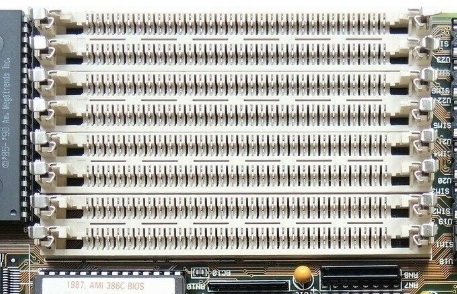 The motherboard has eight 30-pin SIMM slots, split into 2 banks of 4 slots each - this banking is because the 386DX and 486 are 32-bit CPUs, so the external bus width is also 32 bits wide, and since 30-pin SIMMs are 8 bits wide, we need 4 of them to fill a bank (8 x 4 = 32). Bank 0 is the top 4 slots closest to the edge of the board, and Bank 1 is the bottom 4 slots closest to the BIOS chip. Bank 0 must be fully occupied otherwise the board will not work.
The maximum amount of memory supported by the EXP3406 is 64 MB, which was a huge amount even for 1994. Even the highest-end PC only got 16 MB of RAM that year, so this board definitely offered good scope to expand, though hampered by the slow 8-bit SIMMs.
The slots accept all the standard 30-pin SIMM modules: 256 KB, 1 MB, 4 MB and 16 MB (no 8 MB), though apparently they must be parity SIMMs.
The various memory configurations it will support are:
| Bank 0 modules | Bank 1 modules | Total Memory |
|---|---|---|
| 256 KB | empty | 1 MB |
| 256 KB | 256 KB | 2 MB |
| 1 MB | empty | 4 MB |
| 1 MB* | 256 KB* | 5 MB |
| 1 MB | 1 MB | 8 MB |
| 4 MB | empty | 16 MB |
| 256 KB** | 4 MB** | 17 MB |
| 1 MB | 4 MB | 20 MB |
| 4 MB | 1 MB | 20 MB |
| 4 MB | 4 MB | 32 MB |
| 16 MB | empty | 64 MB |
*The chipset datasheet has these two reversed, so 256 KB in Bank 0 and 1 MB in Bank 1.
**The chipset datasheet does not have this configuration.
The seller was kind enough to include four SIMMs installed on the board. These are NEC branded, gold-plated parity FPM (Fast Page Mode) ones rated at 70ns, which is about as fast as 30-pin SIMMs went. 80ns was much more common, and 60ns SIMMs did exist but were horrendously incompatible until 72-pin (32-bit) SIMMs arrived. By default, the BIOS is setup with 2 wait states for memory reads, and 1 wait state for memory writes with this CPU.
Level 2 Cache
According to the user manual this board supports up to 256 KB of L2 cache - two banks of up to 128 KB in each. It was common for late 386 motherboards to get some amount of L2 cache to help provide a minimum accepted level of performance while retaining a budget price point in the PC market.
This OPTi chipset's onboard cache controller uses a bank-interleaving scheme if both banks are in use, which can significantly improve performance, so is highly recommended especially if using a 486 upgrade chip on this board (486-class systems benefit much more from having a L2 cache than 386s). Cache Bank 0 is the one closest to the corner of the motherboard and Cache Bank 1 is the one closest to the SIMM slots.
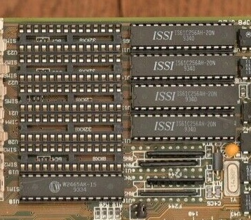
Bank 0 contains 128 KB of L2 cache
in four ISSI 20ns SRAM chips, plus a Winbond 15ns Tag RAM chip.
Bank 1 is empty.
Interestingly, looking in the datasheet for the chipset, it says it can support L2 cache sizes of 32 KB (386 mode only) and 512 KB as well (486 mode only).
It also says that cache sizes of 128 KB and 512 KB are single bank caches, so the interleave scheme would not be used, while 64 KB and 256 KB are double-banked which would use the interleave scheme.
The available cache configurations according to the user manual are:
| L2 Cache Size | Bank 0 (U12-U15) | Bank 1 (U20-U23) | Tag RAM | Cacheable Main Memory |
|---|---|---|---|---|
| 64 KB | Four 8K x 8 | Four 8K x 8 | U18=8K x 8, U19=empty | 16 MB |
| 128 KB | Four 32K x 8 | empty | U18=8K x 8, U19=empty | 32 MB |
| 256 KB | Four 32K x 8 | Four 32K x 8 | U18=8K x 8, U19=8K x 8 or U18=32K x 8, U19=empty |
64 MB |
The chipset datasheet gives these additional cache configurations, which I will have to try out!
| L2 Cache Size | Bank 0 (U12-U15) | Bank 1 (U20-U23) | Tag RAM | Cacheable Main Memory |
|---|---|---|---|---|
| 32 KB | Four 8K x 8 | empty | U18=8K x 8 | 8 MB |
| 512 KB | Four 128K x 8 | empty | U18=32K x 8, U19=empty) | 64 MB |
In terms of cache chip speeds, it is recommended that 25ns SRAM and Tag RAM chips be used if the CPU speed is 25 MHz or slower. For 33 MHz and higher clock speeds, use 20ns for the cache SRAMs and 15ns for the Tag RAM(s). SIMMs for the main memory should be 80ns.
My board came with 128 KB of 20ns SRAMs with a 15ns TAG RAM chip - perhaps boards that got the 486SX soldered in came with the slower cache chips. I have bought some more 32 KB SRAM chips in order to get some performance timings from this board with 256 KB of L2 cache, but also some 128 KB SRAM chips to see if the chipset datasheet's 512 KB is possible, even though this is kind of pointless given that 256 KB of L2 cache is sufficient to make the full 64 MB of main memory cacheable.
BIOS
The EXP3406 typically uses an American Megatrends (AMI) BIOS. Looking around the web, the following AMI BIOS strings have been identified on various revisions of this board:
40-04AA-001107-00101111-111192-OP495SLC-F (dated 11th November 1992)
40-040C-001117-00101110-080893-OP495SLC-F (dated 8th August 1993)
My motherboard however, uses an Mr BIOS (Microid Research) version 1.60 and dated 26th January 1994 (download it here). Enthusiasts generally say Mr BIOS' are an upgrade on AMI or Award BIOS, offering better performance, more flexibility and options for overclocking. Getting into the BIOS is done by pressing ESC during the memory test, or once the system has started by pressing Ctrl-Alt-ESC - that's a very nice feature to have!
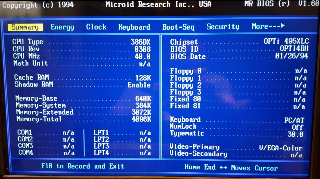
The Summary page indicates our Am386DX-40 with 128 KB of L2 cache
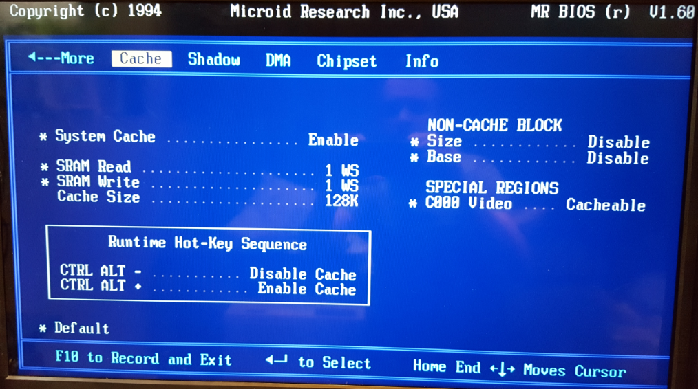
The Cache page shows the BIOS defaults to 1 wait state for both reads and writes
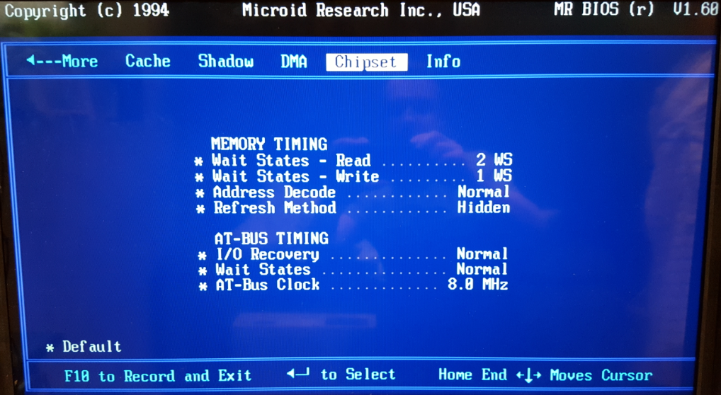
On the Chipset page, it defaults to quite a lot of wait states on main memory
In part 2 I will explore some expansion options, so keep checking in over the coming weeks for an update! **UPDATE: Click here for part 2! **