 Retro Review: Lucky Star 5I-TX2A Motherboard - Part 1
18th April 2025
I recently acquired this Intel 430TX-based motherboard from 1997 as part of a bundle. The main item I wanted was actually the Yamaha Audician 32 Plus with the onboard wavetable synth (I previously reviewed another of these cards without the wavetable).
Anyway, it came with this motherboard along with an IBM 6x86MX PR233 CPU, the sound card, and a UMC 16-bit ISA VGA card.

Lucky Star 5I-TX2A "Lyra" ATX motherboard (1997)
Lucky Star were known in the 90s along with many other Taiwanese manufacturers as producing cheap-quality motherboards for the masses of non-brand off-the-shelf PCs. This one is the 5I-TX2A (codenamed "Lyra"), which is roughly translated as 5th-generation CPU and Intel 430TX Triton II chipset.
In 1997 Intel was becoming a big player in the PC motherboard chipset market, and coupled with the brand new Pentium II in the new "Slot 1" format, mid-range PCs this year typically came with a fast Pentium MMX or an AMD/Cyrix/IBM instead such as a Cyrix [or IBM like the one in my bundle] 6x86 MX running on a Socket 7 motherboard like this one. Memory-wise, a typical PC came with between 8 MB and 32 MB of RAM using either old 30-pin SIMMs, 72-pin SIMMs, or the latest 168-pin DIMMs which ran at the same speed as the Front Side Bus.
The Lucky Star 5I-TX2A, like other Taiwanese motherboards, was designed to suit the broadest market available, and this was their latest Socket 7 offering for mid-to-late 1997. It supported all the popular Socket 7 CPUs and both 72-pin as well as the new 168-pin DIMM memory. Note that this isn't a 'Super Socket 7', as there's no support for AGP or 100 MHz FSB here.
It's very similar to most of their earlier 430TX-based boards, all of which were released in 1997. Here's a summary of Lucky Star's TX-based motherboards:
| 5I-TX12 | 5I-TX1A | 5I-TX1B | 5I-TX1C | 5I-TX2A | |
|---|---|---|---|---|---|
| Board Size | Baby AT (254x218) | Baby AT (254x218) | Baby AT (254x218) | Baby AT (254x218) | Micro ATX (220x190) |
| Chipset | i430TX Triton II | i430TX Triton II | i430TX Triton II | i430TX Triton II | i430TX Triton II |
| L2 Cache | 256 KB or 512 KB | 256 KB or 512 KB | 256 KB or 512 KB | 256 KB or 512 KB | 256 KB or 512 KB |
| FSB Speeds | 50, 60, 66 | 50, 55, 60, 66, 75* | 50, 55, 60, 66, 75* | 50, 60, 66 | 50, 55, 60, 66, 75* |
| CPU Vcore | 2V - 3.5V | 2.8V - 3.5V | 2V - 3.5V | 2V - 3.5V | 2V - 3.5V |
| Expansion slots | 3x ISA, 4x PCI | 4x ISA, 3x PCI | 4x ISA, 4x PCI | 3x ISA, 4x PCI | 3x ISA, 4x PCI |
| Memory | 4x 72-pin, 2x 168-pin | 4x 72-pin, 1x 168-pin | 2x 72-pin, 2x 168-pin | 4x 72-pin, 2x 168-pin | 2x 72-pin, 2x 168-pin |
| Maximum RAM | 128 MB | 128 MB | 128 MB | 128 MB | 256 MB |
| Power Conn. | AT and ATX | AT only | AT and ATX | AT and ATX | AT and ATX |
| Integrated Peripherals | 2x IDE, 1x floppy, 2x serial, 1x parallel, 2 x USB, 1 x PS/2 |
2x IDE, 1x floppy, 2x serial, 1x parallel, 2 x USB, 1 x PS/2 |
2x IDE, 1x floppy, 2x serial, 1x parallel, 2 x USB, 1 x PS/2 |
2x IDE, 1x floppy, 2x serial, 1x parallel, 2 x USB, 1 x PS/2 |
2x IDE, 1x floppy, 2x serial, 1x parallel, 2 x USB, 1 x PS/2 |
| BIOS | Award | Award | Award | Award | Award |
So the key improvement with the TX2A here is its support for 256 MB of RAM - everything else is the same as for the earlier TX1B, except the 1B got the additional ISA slot.
Given that Socket 7 is backward-compatible with Socket 5, this board should be a good choice if you're into playing old DOS games from 1993 through to the Windows 95/98 era up to 1999. It's not the first budget board I've reviewed (see the PC Chips ones in the reviews list), so it will be interesting to see what it's capable of....
Quick Visual Inspection
Looking around the board it appears to comprise the following:
|
The board layout on this V1.0 revision (the only revision I've found) is very tight, and one of the ISA slots is shared with the nearest PCI slot, so both cannot be used at the same time.
Date-wise, the most recent date stamp on the motherboard's chips is week 41 of 1997, and most of the chips are only a few weeks earlier. This date stamp puts the motherboard's manufacture in the week of 6th October 1997.
The Component Parts
The CPU Socket
 Being a Socket 7 motherboard it supports split-rail voltage CPUs, though it doesn't cater for the older 5V-only CPUs like the original Pentium P5 chips. You do have to set jumpers on these motherboards to reflect the CPU installed. I've seen worse though - on these boards you have five jumpers to configure the CPU type, Vcore voltage, FSB speed and clock multiplier - the available CPU options are listed below, with clock speeds ranging from 75 MHz up to 233 MHz according to the manual:
- Intel Pentium (P54C) 75-200 MHz
- Intel Pentium MMX (P55 and P55C Overdrive) 166-233 MHz
- AMD K5 PR75-PR166
- AMD K6 PR166-PR233
- Cyrix/IBM Cx6x86 M1 P133+ to P200+ (both the earlier 3.52V ones and 6x86L which ran at 2.8/3.3V)
- Cyrix/IBM Cx6x86MX PR166-PR233
Not documented in the manual but still supported through one of the above configurations are:
- IDT WinChip 2 and 2B
- IDT WinChip C6
- AMD K6-II/+ and K6-III/+
The Chipset
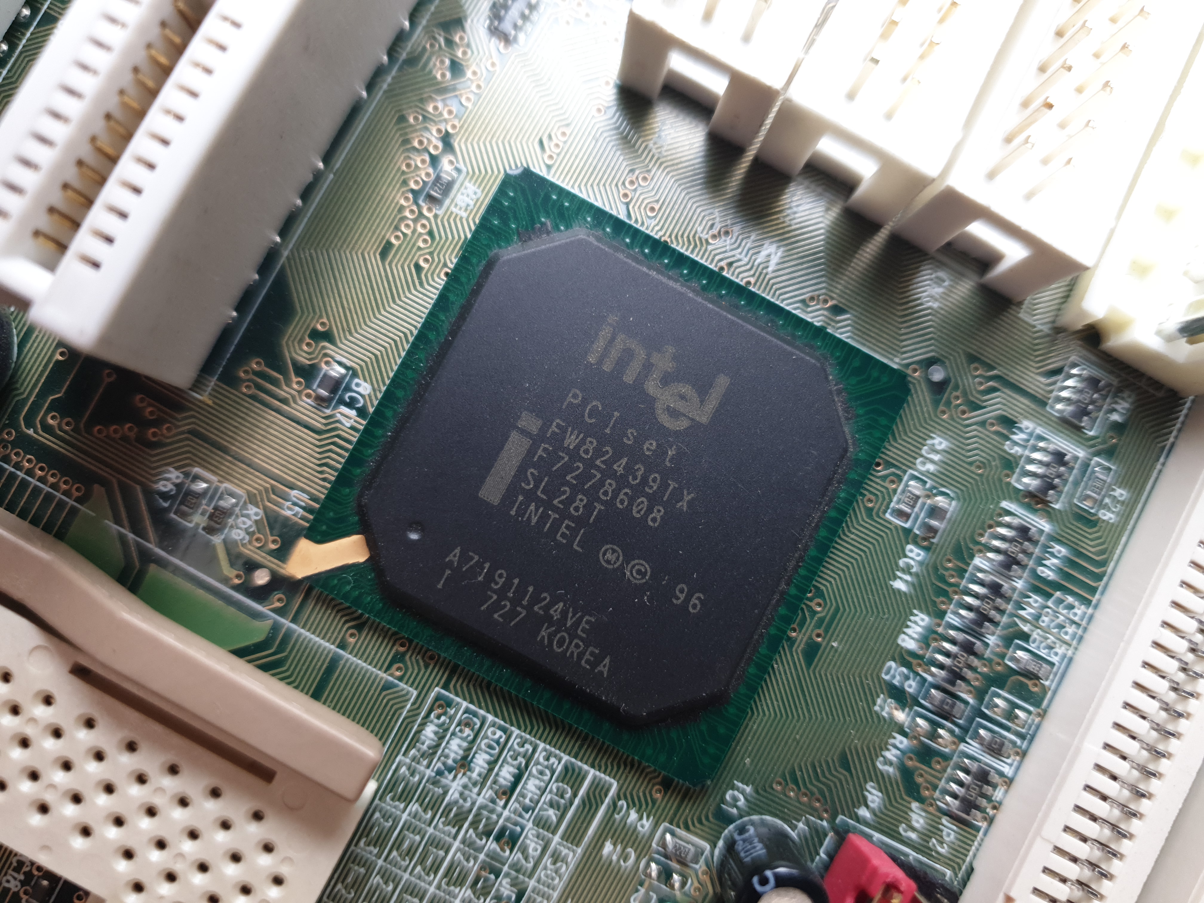 The Intel 430TX "Triton II" chipset was made up of two chips: the 82439TX system controller (Northbridge) and 82371AB peripheral controller (Southbridge). It was supposed to be their final Socket 7 chipset, superceding the capabilities of the earlier excellent 430FX "Triton I" and 430HX (confusingly also called "Triton II"). The 430HX gave us USB support as well as up to 512 MB of main memory, all of which could be cached. The main issue with the HX was its high cost, and many motherboard manufacturers cut corners by choosing to fit a degraded Tag RAM chip which only enabled the first 64MB of RAM to be cached instead of the maximum 512MB. Apparently the 430TX was the same in this regard.
Its southbridge PIIX3 IDE Controller is considerably faster than the PIIX controller found in the FX Triton I chipset, and it added support for the UltraDMA specification, UDMA/33. The 430TX was also the first chipset to unofficially support the 83.3MHz bus frequency that started to appear in 1997.
Memory
 The Lucky Star 5I-TX2A provides two 72-pin SIMM slots and two 168-pin DIMM slots. The former takes only the slightly faster Extended Data Out (EDO) SIMMs, not the older Fast Page Mode (FPM) modules.
The new DIMM slots use the much faster SDRAM which uses 5-1-1-1 timing at 66 MHz FSB. The board supports (and of course the manufacturer recommends) the use of PC66 or PC100 DIMMs. Because DIMMs are driven at the same frequency as the Front Side Bus, you must use PC100 DIMMs if you configure the BIOS to use a FSB frequency of 75 MHz to get the best performance.
The 168-pin DIMM slots make up 'Bank 0' and 'Bank 1' (bank 0 is closest to the 72-pin SIMM slots and bank 1 is closest to the edge of the board) - you can populate just Bank 0 or both (or none if you're only using the 72-pin slots). They take 8 MB, 16 MB, 32 MB, 64 MB, and 128 MB DIMMs (there is no support for 256 MB DIMMs).
The two 72-pin SIMM slots make up 'Bank 2', and accept 8 MB, 16 MB, 32 MB, 64 MB and 128 MB SIMMs.
It has been suggested by some that you can only use either the 72-pin SIMM slots or the 168-pin DIMM slots, not both at the same time. That would make sense, given the performance differences between the two technologies, but I will test this out anyway for the record. I imagine the SDRAM DIMMs would be throttled back massively to run at the same speed as the SIMMs.
Also note that the DIMM slots support both 5V and 3.3V modules, selectable via jumper JP1 to the right of the upper SIMM slot (jumpering the top two sets of pins for 3.3V, the lower two sets for 5V). This is to cater for the earliest DIMM modules which came with FPM or EDO memory and these required a 5V supply to operate. If your DIMM module has SDRAM chips you need to set this board's memory jumpers to the "3.3V" setting.
Level 2 Cache
 By 1997, the days of having SRAM cache sockets were gone. The cost of static RAM was coming right down, so motherboards tended to come with soldered-in cache chips of whatever the maximum the chipset supported. In the case of the 5I-TX2A here, we have two MoSys MC80164K32Q-75 chips. These are configured as 64K x 32 [bit], and hold 256 KB each, giving us a decent Level 2 cache size of 512 KB.
The tag RAM chip used here is an ISSI IS61C256A, which is a 32Kx8 chip - perfectly suitable for up to 64 MB of main memory with this 512 KB L2 cache in writeback mode, or 128 MB of main memory in write-through mode.
BIOS
 My motherboard came with an Award PCI/PNP 586 flash BIOS which is the very common v4.51PG. It has a BIOS string of 10/28/97-i430TX-2A59IL1CC-00.
In Lucky Star's lingo, this tells me this is BIOS version O2-000, which is one of the earlier ones. Strangely, the BIOS string's date doesn't match the BIOS version of O2-000 - the date is 1.5 months later, and just 1 day before the known O2-002 BIOS date. I'll be sure to dump my BIOS and do a comparison of its contents to some of these others.
Known BIOS versions for the 5I-TX2A are:
- O1-000: dated 12th August 1997. BIOS string = 08/12/97-i430TX-2A59IL1CC-00. No other text shown.
- O2-000: dated 12th September 1997. BIOS string = 09/12/97-i430TX-2A59IL1CC-00. Text shown: P54/P55C 97/10/27 O2-000 AT/ATX
- O2-002: dated 28th October 1997. BIOS string = 10/28/97-i430TX-2A59IL1CC-00. No other text shown.
- O2-004: dated 27th November 1997. BIOS string = 11/27/97-i430TX-2A59IL1CC-00. Text shown: P54/P55C 97/12/22 O2-004 AT/ATX
- O2-006: dated 11th June 1998. BIOS string = 06/11/1998-i430TX-2A59IL1CC-00. No other text shown.
(1) The 32GB bug - when a disk larger than 32 GB is connected the computer hangs after the memory test.
(2) The 64GB Bug #1 - the machine hangs when the output of the Hard disk size is calculated in the information table (CPU, Clock, hard disks 1-4, cache, memory ...)
(3) The 64GB bug #2 - when calling the IDE Auto-detection in the BIOS, the computer hangs.
Fortunately, unofficial fixed BIOS versions exist that remedy these issues. See Jan Hill's site for more information.
The BIOS chip on these motherboards is one of the new flashable ones, in my case a 128 KB Atmel 29C010A, so the BIOS code is upgradable via software after you boot to a DOS prompt or into Windows.
BIOS Boot POST Codes
I sometimes like to know what a working set of POST codes look like for my motherboards - this can help later on when diagnosing problems.
| POST Code | Meaning |
|---|---|
| C0 | Initialise all standard devices with defaults. |
| 00 | ?? |
| C1 | Memory presence test; OEM specific, test the size of on-board memory. |
| C6 | Cache presence test; External cache-size detection test |
With CPU and memory installed (no video card, no keyboard), the board remained on POST code C6 with 1 long beep that repeated. This was due to a memory module issue - reseating the DIMM and rebooting got rid of the error and the BIOS proceeded.
Now, with the same configuration (still no video card or keyboard), 1 long beep, 3 short (indicating no video card), we get this:
| POST Code | Meaning | More info |
|---|---|---|
| C0 | Initialise all standard devices with defaults. | |
| 00 | Reserved | |
| C1 | Memory presence test; OEM specific, test the size of on-board memory. | |
| C6 | Cache presence test; External cache-size detection test | |
| 0C | Initialize keyboard; Detect the type of keyboard controller | Keyboard LEDs flash once |
| C3 | ?? | |
| C5 | Early shadow; OEM specific, early shadow enable for fast boot | |
| 03 | Initialize chips; Disable NMI, PIE, AIE, UEI, SQWV. Disable video, parity checking, DMA. Reset math coprocessor. Clear all page registers and CMOS shutdown. Initialize DMA controller 0 and 1. Initialize interrupt controllers 0 and 1. | |
| 05 | Blank out screen; Clear CMOS error flag | |
| 06 | Reserved | |
| 07 | Clear 8042 interface; Initialize 8042 self test | |
| BE | Chipset default initialization; Program chipset registers and power-on BIOS defaults. | |
| 09 | Early cache initialization; Cyrix CPU specific, CPU and cache initialization | |
| 0A | Set up interrupt vector table; Initialize first 120 interrupt vectors | |
| 0B | Test CMOS RAM checksum | |
| 0D | Initialize video interface; Detect CPU clock, read CMOS location 14h to find the type of video in use, detect and initialize video adapter | Video now shown |
| BF | Chipset initialization; Reserved | |
| 0D | Initialize video interface; Detect CPU clock, read CMOS location 14h to find the type of video in use, detect and initialize video adapter | 1 long, 3 short beeps (no video card) |
| 0E | Test video memory; Write sign-on message to screen, setup shadow RAM | |
| 0F | Test DMA controller 0; BIOS checksum test, keyboard detect and initialization | |
| 14 | Test timer counter 2 | |
| 15 | Test 8259-1 mask bits | |
| 16 | Test 8259-2 mask bits | |
| 18 | Test 8259 interrupt functionality | |
| 19 | Test stuck NMI bits (parity I/O check) | |
| 30 | Size base and extended memory; Size the base memory from 256K to 640K and the extended memory above 1MB | |
| 31 | Test base and extended memory; Test the base memory from 256K to 640K and the extended memory above 1MB using various bit patterns | |
| 32 | Test EISA extended memory | |
| 35 | Reserved | |
| 3D | Initialize and install mouse if present | |
| 3E | Setup cache controller | |
| BF | Chipset initialization; Reserved | |
| 42 | Initialize hard drive | |
| 43 | Detect & Init. serial & parallel ports | |
| 45 | Detect and Init. math coprocessor | |
| 4A | Reserved | |
| 49 | Reserved | |
| 4B | Reserved | |
| 4E | Mfg. POST loop, or display messages | Paused on keyboard error / CMOS checksum error |
After a video card and keyboard are installed, it continues with these:
| POST Code | Meaning |
|---|---|
| 4F | Security password (even if not set) |
| 50 | Write CMOS; Write CMOS back to RAM and clear screen |
| 51 | Pre-boot enable; Enable parity checking, enable NMI, enable cache before boot |
| 52 | Initialize option ROM’s; Initialize and ROM’s present at locations C800h to EFFFFh |
| 53 | Initialize time value |
| 5C | ?? |
| 60 | Setup virus protect (boot sector) |
| 61 | Set boot speed |
| 62 | Setup numlock |
| 63 | Boot attempt |
| FF | End of BIOS POST process |
Testing and First Boot
The initial test hardware I used was what came in the bundle - a nondescript UMC VGA card and an IBM 6x86MX PR233. Oddly, while it appeared to start up without issue, there was no video; my monitor just showed that the signal was out of range ('Unsupported mode'). I then tried another card recently acquired and tested - a Diamond Stealth VRAM - with the same result. Finally, I installed my trusty Tseng Labs ET4000 and it displayed just fine. I'm not yet sure what to make of this... all these 16-bit ISA cards are known to be in working order in another retro PC, and all were tried in each of the three 16-bit ISA slots.
Here's the initial boot-up screen:

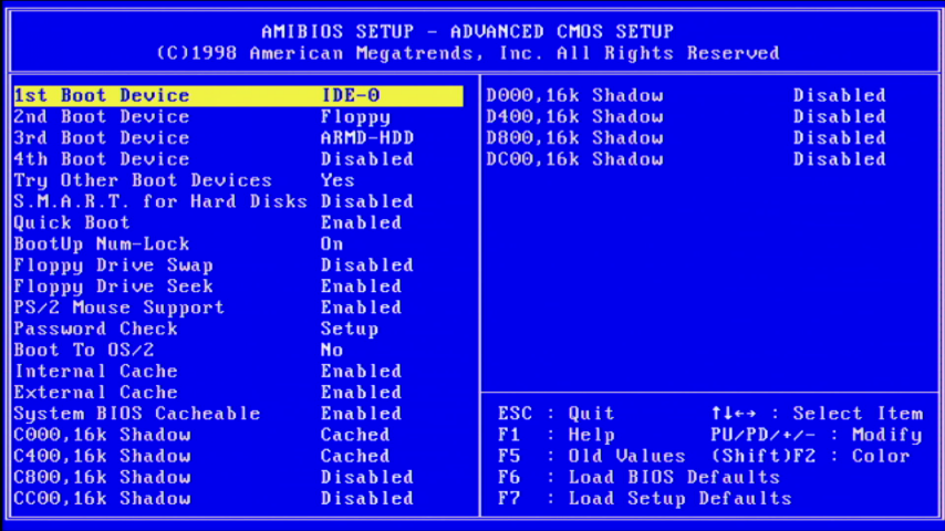
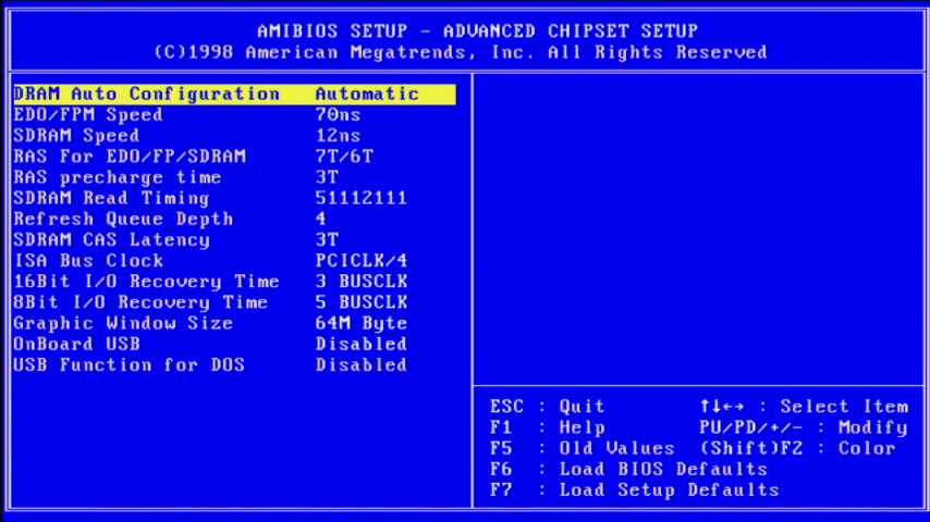
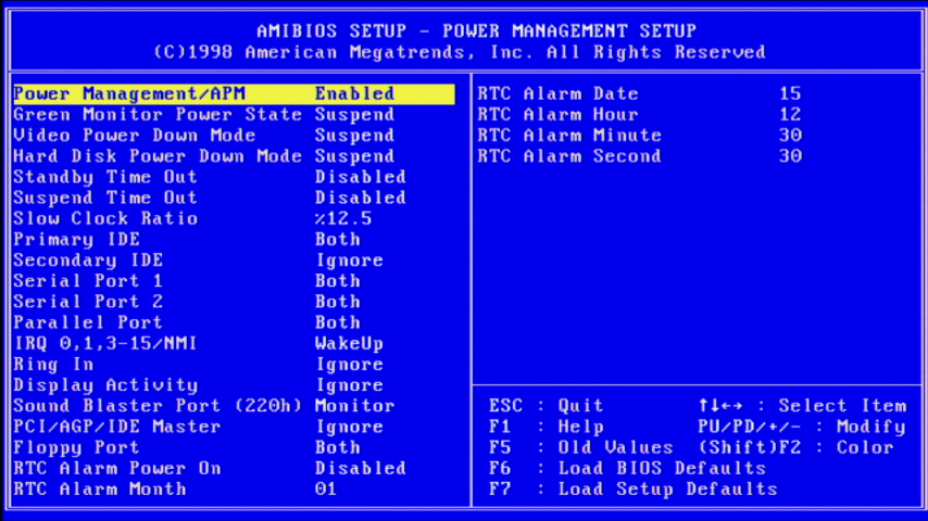
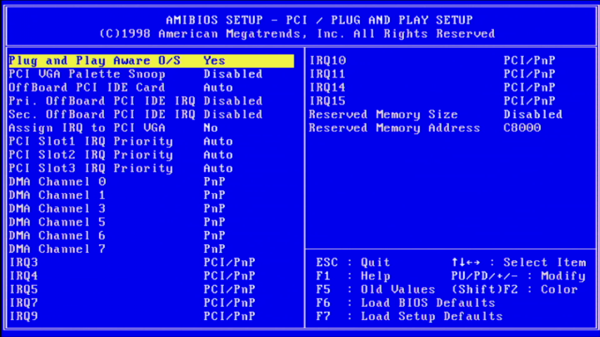
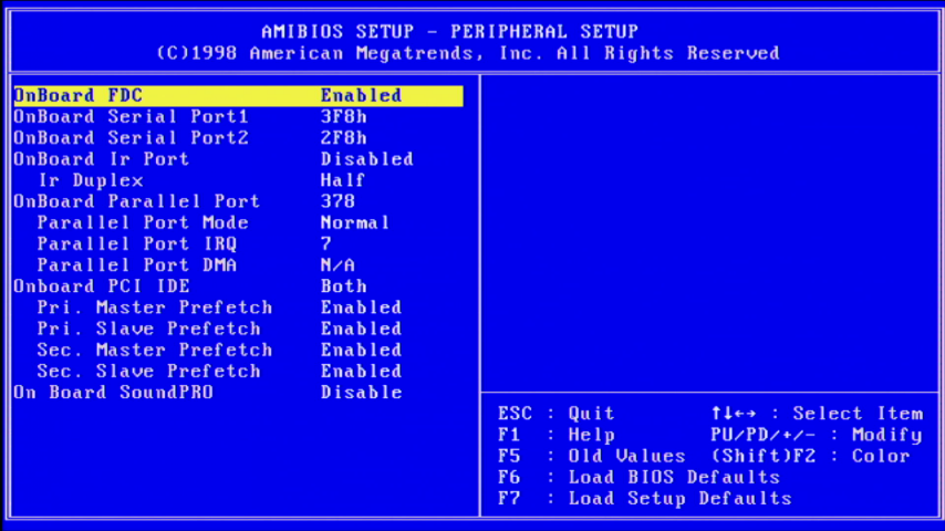
And here are some pics of the various Award 586 PCI/PNP BIOS pages:


Because the CPU type/FSB are set with jumpers, there's nothing in the BIOS to help tweak the CPU / FSB settings, nor can you change the ISA bus speed. Another missing option is to disable the Cyrix CPUID, which is occasionally necessary for compatibility reasons to get software running. Some good memory timing settings though.
In Part 2, we'll get it booting and do some initial testing.