Reviving a Chips & Technologies 386 Motherboard - Part 1
I picked up this great 80386 motherboard from EBay a number of years ago, including an Intel 80386-20 CPU and IIT 3x87 math coprocessor. This review catalogs my findings with this board:
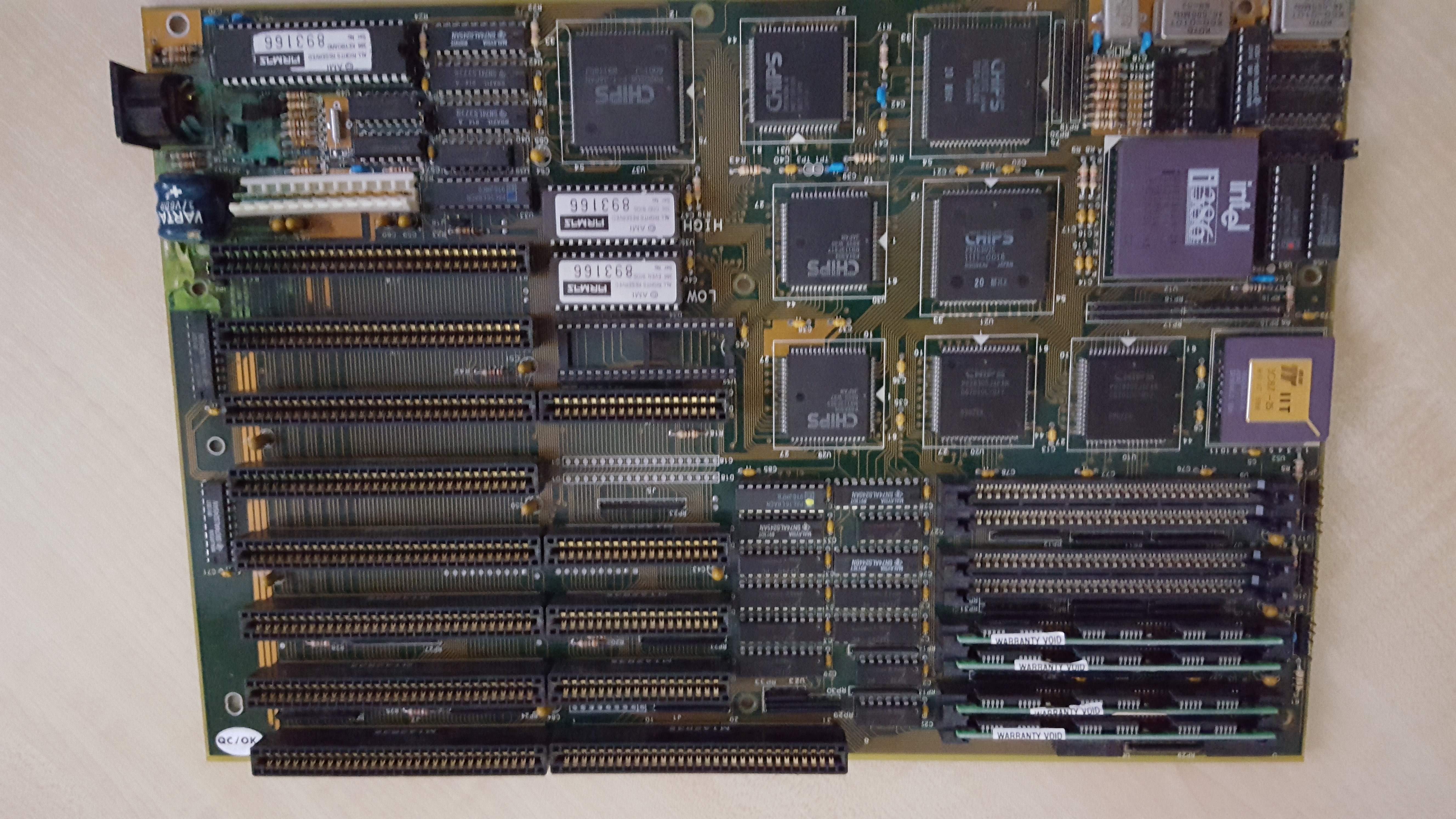
The board has few identifying marks on the silkscreen to indicate its manufacturer or model number, only "MST-1267-A" on the underside, which came up blank when I searched online for it. I initially thought perhaps an early MicroStar board, but their boards always prefixed with MS-, not MST-.
Quick Visual Inspection
Looking around the board it appears to consist of the following:
- A socketed Intel i386-20 CPU. The socket predates socket designations (Socket 1, Socket 2, etc).
- Chips & Technologies chipset (consisting of 8, yes, 8! chips) rated at 20 MHz.
- A socketed IIT 3C87-25 math co-processor.
- American Megatrends Inc. (AMI) BIOS in two chips, and AMI keyboard controller.
- Eight 30-pin SIMM slots.
- Four 16-bit ISA expansion slots, three 8-bit, and one that appears to be proprietary.
- AT P8/P9 power connector
- Full-size DIN keyboard socket
The CMOS backup battery has leaked and caused some corrosion to the main board - this will need to be cleaned up to prevent further corrosion, but aside from that it looks very clean. In the corroded area there are a couple of NPN transistors (ITT3904 and ITT3906), a capacitor, the keyboard socket and even the P9 power connector has 4 of its pins showing signs of the leak, plus surrounding tracks.
Date-wise, the most recent date stamp on the motherboards' chips is week 9 of 1989, so it was certainly no earlier than March 1989 when this was originally sold.
The Component Parts
The CPU
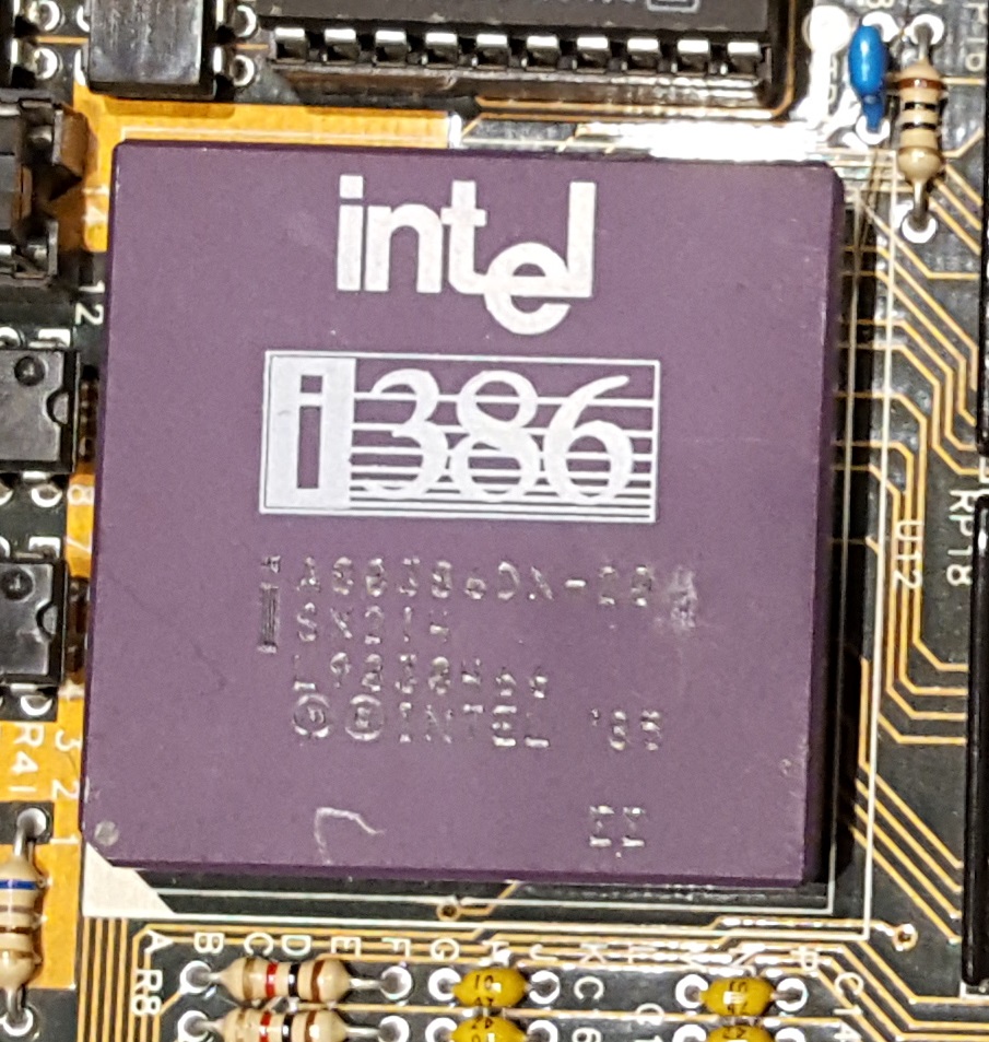 Despite the fact that Intel had launched the 80386 back in 1985, it didn't see widespread consumer use until 1987 or 1988 - it was simply too expensive! In fact the 386DX-20 like I have here would have been installed in nothing less than a "premium PC" in 1987/1988, and it wouldn't be until 1989 that faster 25 MHz variants were seen and even later, 33 MHz.
The double sigma symbol on the lower-right of the chip tells us it passed the 32-bit multiply bug test. The sSpec (sample specification) code for this particular 386 is SX214, which means it's Stepping D. It's in a 132-pin PGA package (pin grid array).
For this CPU, the external bus would also run at 20 MHz, and this is reinforced by the fact that the motherboard has a 40 MHz crystal (the bus would run at CLKIN divided by 2) which can be seen near the bottom-left corner in the top picture.
It's actually quite unusual to see a 386 socketed - many motherboards had their 386 CPUs soldered in (they used the SMT [surface-mount technology] version with teeny-tiny legs), so this suggests to me the motherboard here was high-end when it was sold.
The Chipset
Chips & Technologies always had a premium cachet about them, at least in my memory. The chipset found on this board is the CS8230 386 Chipset, which appears to be a successor to their earlier NEAT (New Enhanced AT) chipset. The chips that make up this CS8230 chipset are as follows:
- P82C206 - Integrated Peripherals Controller (IPC)
- P82A303 - High address buffers
- P82A304 - Low address buffers
- P82A306 - Control signal buffer
- P82B305 - Data Bus Interface
- P82B305 - Data Bus Interface
- P82C301C - CPU/bus controller
- P82C302C - Page/interleave memory controller
So it keeps the same P82C206 IPC chip as the NEAT chipset, but the others are different.
The chips themselves have a MHz rating stamped on the top of some of them, 20 MHz in this case. This was quite common at the time, as these VLSI (Very Large Scale Integration) chips were considered quite sensitive (indeed, some 386 boards had these socketed for easier replacement), and overclocking them would usually result in permanent damage to the chip. So I know it would be foolish to put a faster 386 CPU and crystal(s) this time around.
The BIOS in this 386 was really not designed for consumer tweaking - it existed so that OEMs and third-party system builders could adjust the PC's performance to suit the specific hardware they were installing, such as the CPU, memory capacity and speed, etc. The chipset allows us to configure the CPU and AT bus's clock rates, as well as memory and I/O wait states ("No-Operation" commands - basically delays). DRAM type, shadow RAM capability and DMA wait states can also be programmed. The 82C206 IPC chip mentioned above is the one that also contains the CMOS RAM memory used to store the chipset configuration.
MEMORY
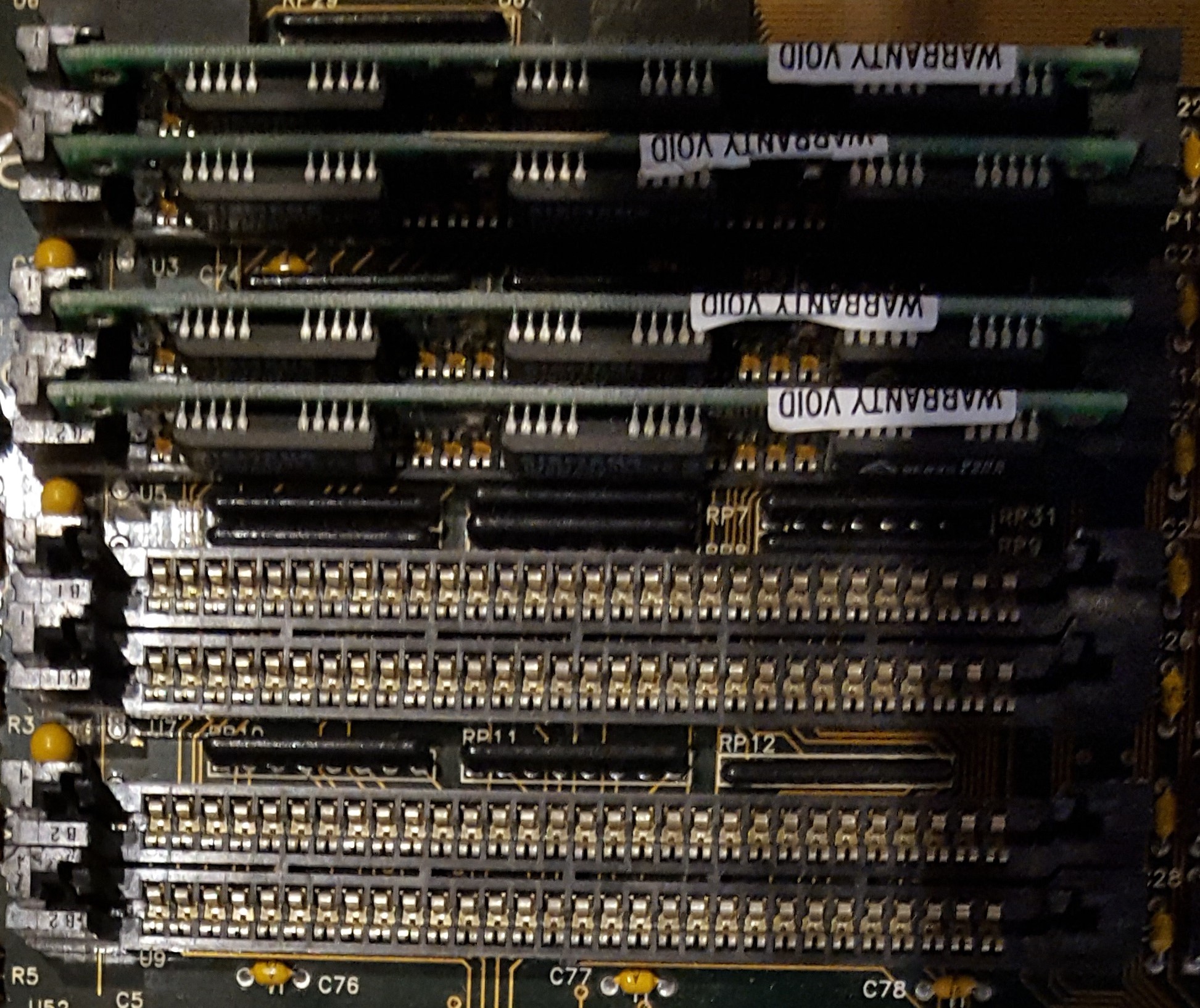 The motherboard has eight 30-pin SIMM slots, split into 2 banks of 4 slots each - this is known because the 386 is a 32-bit CPU, so the external bus width will also be 32 bits wide, and since 30-pin SIMMs are 8 bits wide, we need 4 of them to fill a bank (8 x 4 = 32).
I reckon the maximum amount of memory supported by this board is 8 MB, which is a huge amount for the time when it was purchased. 2 MB on a 386 would have been considered mid-range in 1989, and 4 MB high-end, so this motherboard was designed with future expansion in mind.
Unlike some later motherboards that also supported 30-pin SIMMs, this one doesn't have the nice angled insertion brackets that click the memory into place. Instead, you simply have to align the SIMM card into the slot vertically, using the plastic guide rails on each end, and push down. Still, at least they're SIMM slots rather than SIPP as I have lots of 30-pin SIMMs lying around but no SIPPs.
Extraction is probably more difficult than insertion. I tend to make use of the drilled holes at each end of the SIMM card, and using a small watchmaker's screwdriver I lever up the card from the slot using the pillars of the plastic guides for leverage.
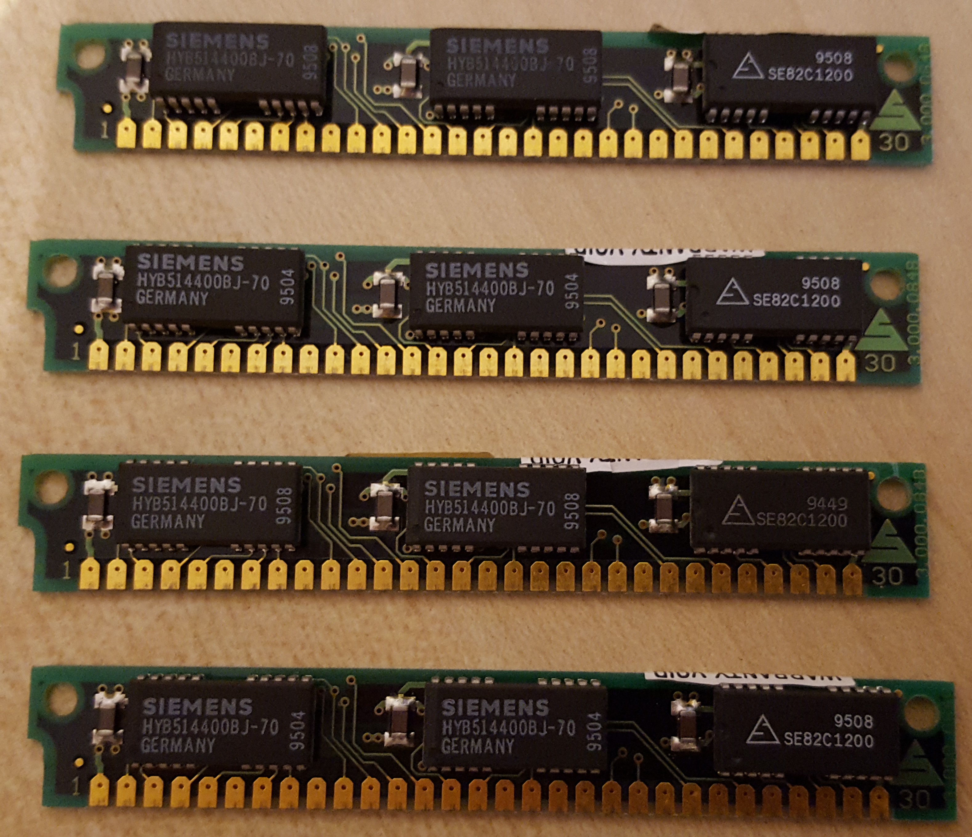
This is the memory I'm going to use, at least initially.
Four 30-pin SIMM modules with ICs manufactured by Siemens, each of which has 1 MB of memory. The memory chips are 70ns so nice and fast for this 386 system!
JUMPERS
The 386 motherboard has a number of jumpers, which at the moment I really have no clue what they do. With the board properly booting, they are setup as follows:
| Jumper | Setting | Location |
|---|---|---|
| JP1 | open | By front panel connectors |
| JP4 | 2-3 short | Just above backup battery |
| JP6 | 1-2 short | Below and to left of P8/P9 power connectors |
| JP? | 2-3 short | Below and to right of P8/P9 power connectors |
| J18 | open | Just to left of P8/P9 power connectors |
| J21 | 1-2 short | Below and to right of P8/P9 power connectors |
Other test hardware
For video, I turn to one of my trusty Cirrus Logic CL-GD510/520 auto-switching Super VGA cards. This card is rock solid and supports all graphics standards natively (hardware emulation) - I'll do a separate review of these cards at some point because they really are the most versatile and compatible around. Hercules, CGA, EGA, VGA and SVGA - all software simply sees a graphics card of the standard configured by the 8 DIP switches.
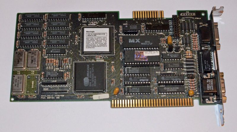
This is actually my other (smaller) CL video card, but functionally it's identical to my older, longer card.
For testing I'm going to use an ATX 400W PSU from an old Pentium 4, coupled with an ATX-to-AT adapter. You can pick these adapters up inexpensively from various online stores and they come in very handy given the rarity of AT-style power supplies these days. Some varieties come with a power switch while others come with female blade connectors that must be shorted for power to be drawn.
And now for an intermission...
*** WARNING: I take no responsibility for any harm or loss caused to anyone as a result of reading these pages and messing about with a PC's innards or the power supply that feeds it - if you're not a qualified electrician I recommend you don't touch it! ***
..and back to the programme, This gives me the P8 and P9 connectors that the board requires:
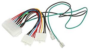
Remember the golden rule for most IBM PC-compatible AT PSU connectors: when connecting the P8 and P9 connectors into the motherboard, always have the BLACK WIRES TOGETHER*.
*Thanks to Piotr Zurawski who wrote in to inform me that some PC compatibles from mainstream manufacturers, including this Tandon 286, do not use the standard P8 and P9 connector pinouts, despite still having two 6-pin connectors! Always check your motherboard or computer manual to be sure.
READY FOR POWER ON?
So I think I have everything I need... The motherboard with CPU and memory installed, a graphics card installed in one of the ISA slots, P8/P9 motherboard power connectors being fed from a modern ATX power supply, and an AT keyboard with old-style DIN plug.
The monitor I will be using to test is a CRT I bought used from an EBay seller a while back for £95 - it's a ViewSonic G75f 17" multisync monitor which produces a nice clear picture with 0.21mm dot pitch (remember when that was a key selling point?) and supports resolutions far beyond what we'll be seeing! For screenshots I may have to reconnect an LCD monitor to avoid them showing vertical scan lines and moire effects.