Retro Review: nVidia Geforce 256 DDR Part 1
1st March 2025
This week I finally got my hands on an nVidia Geforce 256 graphics card. It's one that has been on my wanted list for a long time and was generally considered to be a real turning point in the graphics card market upon its arrival in late 1999, especially for 3D gaming.
Special thanks to DOS Days' regular contributor, targeted for finding this card, paying for it upfront, and then shipping it onward to me.


Creative Labs 3D Blaster Annihilator Pro, model CT6970 (1999)
Thinking this was going to be the original Creative Annihilator which uses SDR (single data rate) SDRAM, I was pleasantly surprised to find out it's actually the slightly later 'Pro' model with DDR (double data rate) SGRAM. The first version of the GeForce 256 was met with some criticism around its performance, and this was due to its use of SDR memory. The Annihilator Pro arrived about two months later to remedy the situation with its DDR memory. The card wasn't cheap when new - in the UK it retailed for around £200, and in the US, $250 to $270. On average the DDR versions retailed for about $50 more than their SDR counterparts.
Creative had several model numbers for each of their cards. Here's a shortlist of them so we can see where this sits in the line-up:
| Model | Release Date | Description |
|---|---|---|
| CT6940 | November 1999 | 3D Blaster Annihilator for OEM market, 32 MB SDR (166 MHz) memory, 120 MHz core clock, mfr date: 019931-019935 |
| CT6941 | November 1999 | Retail version of the CT6940 |
| CT6960 | ? | 3D Blaster Annihilator, 32 MB SDR (166 MHz) memory, 120 MHz core clock |
| CT6970 | February 2000 | 3D Blaster Annihilator Pro for OEM market, 32 MB DDR 6ns (300 MHz) memory, 120 MHz core clock, mfr date 019942 |
| CT6971 | February 2000 | Retail version of the CT6970 |
| CT6972 | February 2000 | Retail version of the CT6970 |
Creative followed nVidia's reference design to the letter while providing a high-quality fan for cooling. Reference clock speeds per nVidia's recommendations are 120 MHz for the core and 150 MHz for memory, though these cards can be pushed to 135 MHz core and 166 MHz for memory (330 MHz in reality because it's DDR).
The Flypast
So what component parts make up this graphics card? Well it's 1999, so a lot has been condensed onto a single piece of silicon. The card has:
- nVidia GeForce 256 (NV10) GPU with heatsink and fan
- 32 MB of Infinion DDR SGRAM
- SST-branded 128 KB EEPROM for the VGA BIOS
- DE-15 video out on the backplate
- A 2-pin fan header
- Two voltage regulators/MOSFETs
- A 50-pin connector at J1/J2
- Solder pads for what appear to be for DVI and S-Video out
- Bus interface - AGP 2x or AGP 4x with "Fast Writes"
My card came with an interesting, and probably aftermarket cooling fan. A great brand though it is (Papst, known for their quiet operation and reliability), it has a 3-pin cable which is incompatible with the card's onboard fan power header which only has two pins. To get the card running, I had to choose a motherboard with a secondary 'case fan' header to power the graphics card's fan. Slightly worrying though, as this mod could imply the card was run overclocked, possibly shortening its life.
The GPU
 The nVidia GeForce 256 (NV10) has been generally accepted as the first ever GPU (Graphics Processor Unit). What lends credence to this is that it was the first to support Transform & Lighting (T&L) within its chip. Up to this point, this initial process of rendering a scene was the responsibility of the CPU. Calculating the location of the vertices relative to the position of the camera (transform), and the effect of light on the polygon relative to the position of the light source (lighting). This was all done by the CPU, while graphics accelerators such as the 3dfx Voodoo handled only the last part of the pipeline (rasterization) to fill the objects.
With the GeForce 256, the entire 3D graphics pipeline end-to-end could now be done "on-chip", relieving the CPU of this huge burden so it could focus on different jobs. It doesn't sound that impressive, but in 1999 you still needed a very fast CPU to play 3D games - nVidia's new chip meant this was no longer the case (assuming games would take full advantage of it, and with the launch of Microsoft DirectX 7, they did).
The industry took a while to catch up, with most still thinking the brute force approach (faster CPU) was the answer. It wasn't until 6 months later that ATI followed nVidia's approach with the launch of the first Radeon card. 3dfx never released a card with hardware T&L capability.
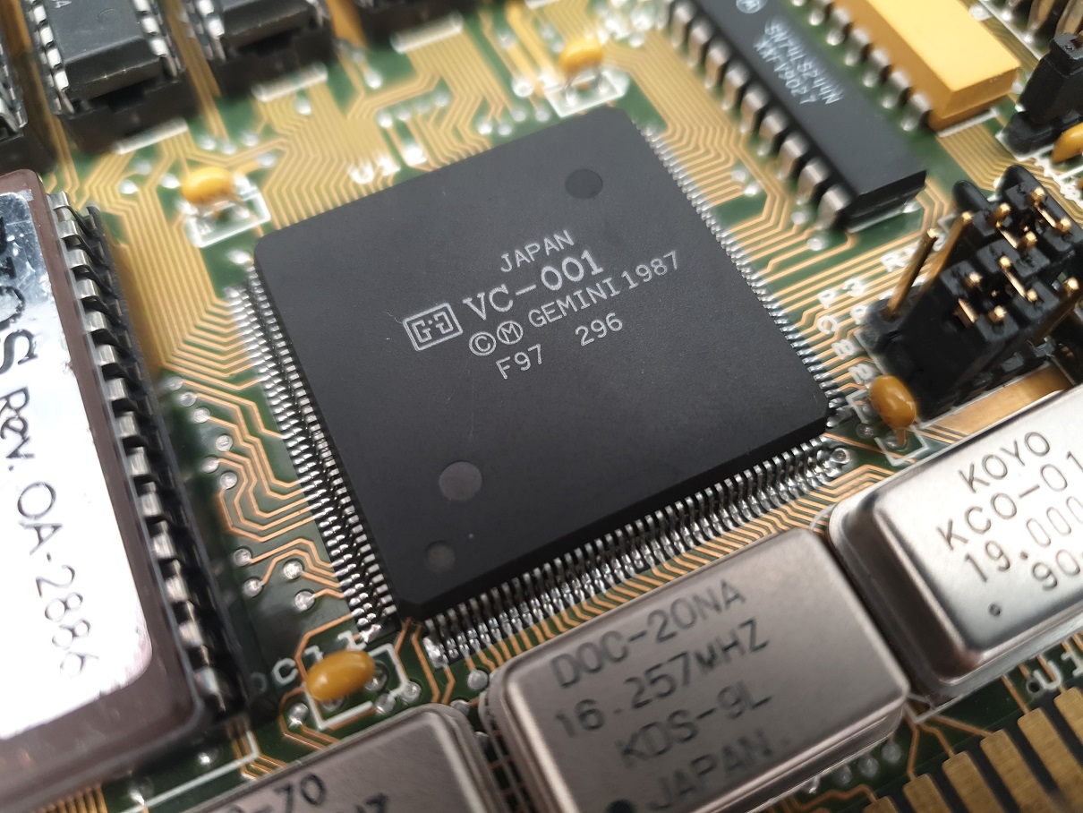
Hidden under both a heatsink and cooling fan, the nVidia NV10
With four rendering pipelines (twice as many as nVidia's previous generation RIVA TNT2), the GeForce 256 pushed the 'fill rate' to 480 Mtexels per second compared to the TNT2's 250. Cards up to this point had mimicked the CPU arms race throughout the 90s - by consistently increasing clock speeds (both core and memory) to cater to the demands of gamers for higher frames per second. This design of the GeForce instead allowed for parallel operations, thus keeping clock speeds reasonably low. The standard core clock speed of the GeForce 256 is 'just' 120 MHz.
The NV10 was also a capable hardware video decoder, with support for MPEG-1 and MPEG-2 with motion compensation.
For software support, the GeForce 256 was designed to work with the most popular APIs of 1999, namely DirectX 7 and OpenGL.
At the time of the GeForce 256's release, no games had been written to make use of DirectX 7's new support for hardware T&L - this hugely computation-heavy task was being undertaken by the CPU, but the fact nVidia provided this hugely advantageous feature caused game developers to start to make use of it.
VGA BIOS
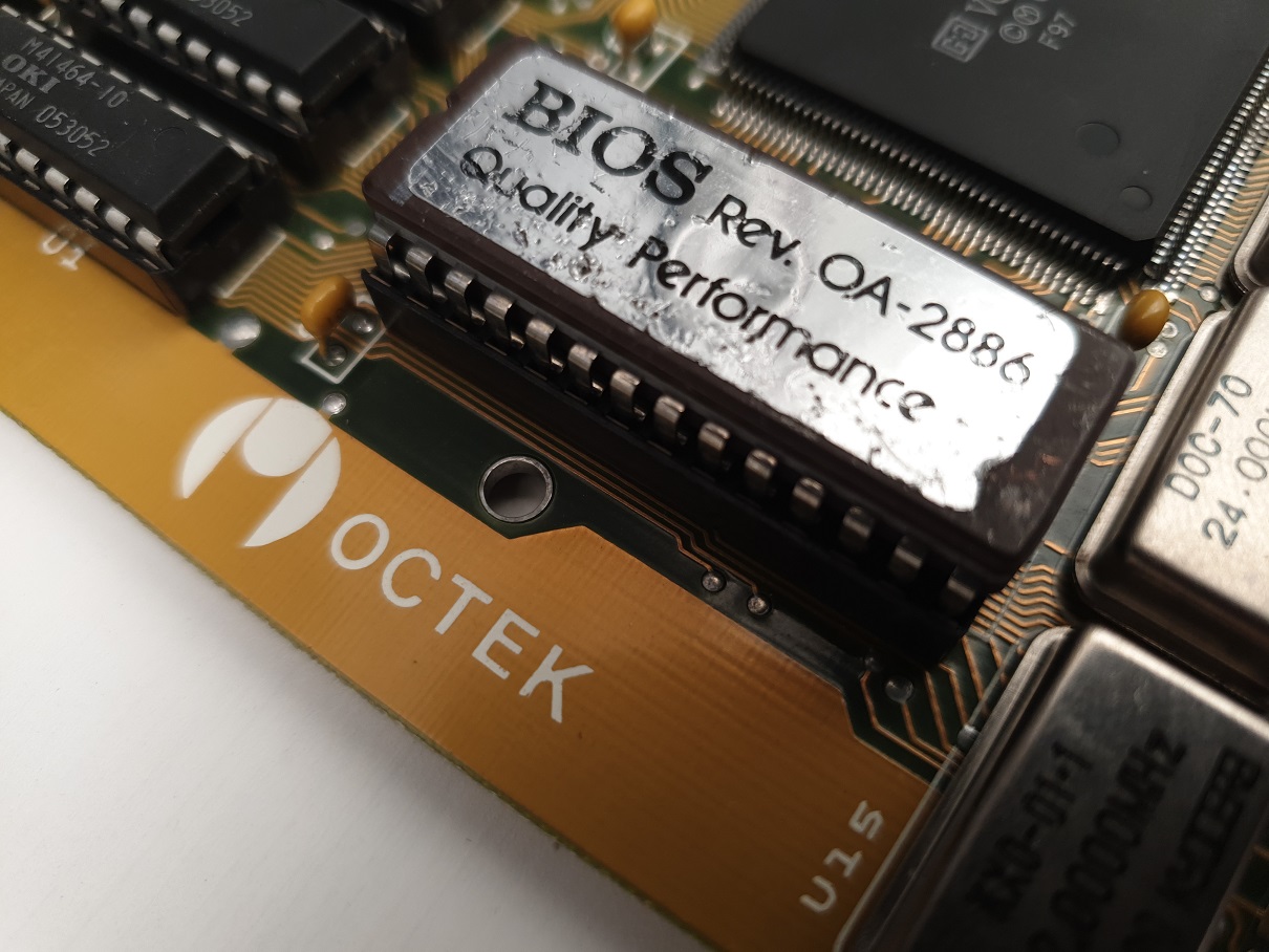 The 128 KB BIOS on the Creative card provides the extended SVGA graphics modes that run 2D resolutions up to 2048 x 1536 in 32-bit colour depth. It is fully compliant with VESA VBE 3.0 too.
The BIOS, being an EEPROM chip, can be overwritten with later firmware. The SST 39VF010 is one of their MPF (Multi-Purpose Flash) range, with advanced overwrite protection, fast reads, and low voltage requirements when writing.
RAMDAC
The RAMDAC is as important as ever on these modern SVGA graphics accelerators as when the first VGA cards first appeared. Its role is to hold colour lookup table data and use it to convert digital colour information into an analogue voltage that represents the various red, green and blue portions of the colour of each pixel for output to the 15-pin VGA output port.
The speed at which the RAMDAC can process this data directly translates to the maximum screen refresh rate the card is capable of. Having lots of video memory coupled to a slow RAMDAC would result in high screen resolutions but with lots of flicker, as these would need to run in an interlaced mode (every odd line drawn first, followed by every even line in a frame) at higher refresh rates or a slower refresh rate in non-interlaced mode (every line drawn in a top-down fashion, also called progressive scan).
Fortunately, the NV10's built-in RAMDAC runs at a blistering 350 MHz, which results in refresh rates up to 240 Hz at the lower resolutions up to 800 x 600 resolution (32-bit colour mode), 200 Hz at 1024 x 768 (32-bit colour mode), and even manages 60 Hz at its maximum resolution of 2048 x 1536 in 32-bit colour mode or 75 Hz in 16-bit colour mode.
Video Memory
 As I mentioned, the Annihilator Pro uses DDR SGRAM memory, effectively doubling the memory bandwidth of the earlier Annihilator that had SDR SDRAM. You can read up on how DDR works elsewhere, but in summary this is achieved by reading/writing to memory on both the high and low edges of a clock cycle, thus managing twice the work each clock.
nVidia's original reference design for the GeForce 256 used SDR that ran at 166 MHz (5.5ns SDRAM chips), and this was recognised early on in the GeForce 256's life after launch as the bottleneck to the chip reaching its full potential. With DDR the difference is very noticeable in 3D gaming with much higher frame rates achievable, especially when running in higher resolutions like 1600 x 1200 where DDR can process its data avoiding the bottleneck that SDR memory would have.
The memory used on the Creative 3D Blaster Annihilator Pro here is Infinion-branded that maxes out at 6ns, so slightly slower than that used on the SDR cards.
AGP Bus Interface
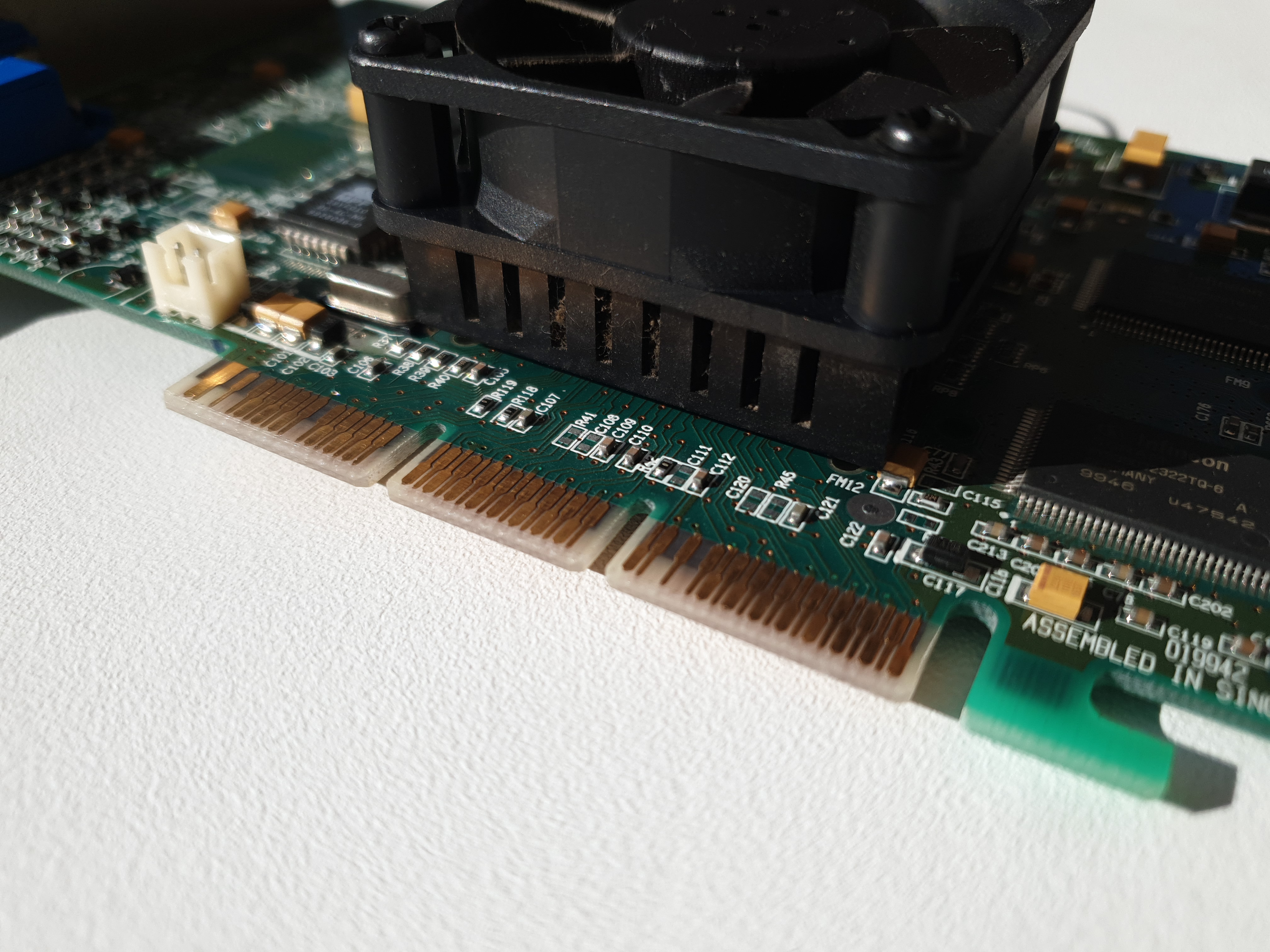 Both the Creative 3D Blaster Annihilator and 3D Blaster Annihilator Pro fully support the AGP 1.0 and 2.0 specification. This means the card is voltage-tolerant, working quite happily in the original AGP 1.0 slot which runs at 3.3V (AGP 2x), or in an AGP 2.0 slot (AGP 4x) which runs at 1.5V.
The card itself has both the 3.3V and 1.5V "keys" in its bus interface edge connector (the leftmost one is the 1.5V key, the right is the 3.3V one). Ordinarily, you need to be very mindful of AGP cards and their slot compatibility, as even though the AGP specification with these keys in the edge connector was sound and should have always prevented incompatible cards being used in the wrong slot, motherboard manufacturers didn't always include these keys to enforce it - bad news if you put a 1.5V-only AGP card in a 3.3V slot!
This voltage tolerance is great, as it means the Annihilator (and Pro) can be used in any AGP 1x, 2x or 4x slot. With AGP 4x you'll get the higher theoretical bandwidth of 1.06 GB/sec, so it's highly recommended you use the card with a motherboard that supports AGP 4x. When running in a slot only capable of AGP 2x this bandwidth is halved, at a theoretical 533 MB/sec, and half that again with AGP 1x.
Furthermore, the GeForce 256 was the only AGP 2.0-compatible card at the time of its release that made use of a special feature that came with the AGP 2.0 specification, "Fast Writes". nVidia released a technical brief explaining the benefits of Fast Writes, which you can read here, but to summarise this feature allows the card to send data from the CPU directly to the GPU without first going through the system memory, where the process is forced to wait as data gets transferred.
The Competition
I will do a full article on the GeForce 256 at some point, but suffice it to say, in late 1999/early 2000, the only real competition that faced the new nVidia chip was from the ATI Rage Fury Maxx, released in October 1999. In some circumstances it could match the base GeForce 256 SDR with its core clock of 125 MHz and memory clock of 143 MHz, but not the DDR-based card. Trailing behind the ATI we also had the Diamond Viper II with its S3 Savage2000, Matrox Millennium G400, and 3dfx Voodoo3 3500.


From left: ATI Rage Fury MAXX, Diamond Viper II, Matrox Millennium G400, and 3dfx Voodoo3 3500
To be honest, you'd be happy playing games on any of these cards unless determined to run everything in 32-bit colour at 1600 x 1200.
Other Versions
The nVidia reference design had provision for both DVI and S-Video outputs alongside the standard DE-15 VGA connector. These would be used in 1999/2000 to be able to connect your PC to a television or flat panel to watch DVDs or other video. My Creative card here just has the solder pads for these ports as well as two missing ICs (a Conexant Bt869KRF video encoder/scaler for the S-Video out and a Silicon Image SI1144 panel controller for the DVI out).
Creative never released a 3D Blaster Annihilator with these features, unlike some of the other graphics card companies who released GeForce 256-based cards. The table below gives you an overview of these competing cards.
| Manufacturer | Released | Details |
|---|---|---|
| ASUS GeForce 256 DDR | February 2000 | S-Video in & out, composite out, 120 MHz core clock, 150 MHz* memory clock |
| ELSA Erazor X2-A32 DDR | January 2000 | S-video out, 120 MHz core clock, 150 MHz* memory clock |
| Hercules/Guillemot 3D Prophet | April 2000 | DVI out, 120 MHz core clock, 150 MHz* memory clock |
| Leadtek WinFast GeForce 256 DDR | January 2000 | S-Video out, DVI out, 120 MHz core clock, 150 MHz* memory clock |
* effectively 300 MHz due to DDR. Tweaking the memory clock shows a range usually from 270 to 330 MHz.
Summary
In Part 2, I will get the card installed along with some Creative or nVidia GeForce 256 drivers running in Windows 98 SE. Once it's ready to go, we'll run some benchmarks and see how it performs with some late 90s 3D games!