BIOS Explained
The BIOS, or Basic Input Output System, is software that is used to define the important configuration aspects of your PC, including the current date and time, and the number and type of floppy and hard drives. It runs immediately after the POST (Power-On Self Test) and before the bootstrap (which locates your boot sector to continue booting the system), reading in these settings to understand what's inside your PC. Your operating system will also communicate to your various hardware devices through the BIOS.
POST
The Power-On Self Test checks the primary hardware devices in your PC, including the CPU, memory, BIOS and any video cards. If a failure is detected at any point, the POST process will halt and produce a series of long and short beeps via the motherboard's PC speaker output to help indicate the root cause of the failure. These beep codes are bespoke to your BIOS manufacturer, and can be looked-up in full elsewhere on the Internet, but here are a few of the more common ones:-
| AMI BIOS 1, 2 or 3 beeps, or 1 long-3 short = Memory 4 beeps = System timer (motherboard) 5 or 7 beeps = CPU 6 beeps = Keyboard 8 beeps, or 1 long-8 short = Video card 9 beeps = ROM (motherboard) 10 beeps = BIOS 11 beeps = Level 2 cache (motherboard) |
Award BIOS 2 short = CMOS setting error 1 long-1 short, or 1 long continous = Memory 1 short continuous = PSU problem 1 long-2 short = Video card 1 long-3 short = Keyboard 1 long-9 short = ROM (motherboard) |
Phoenix BIOS 1-1-1-1, 1-3-1-1, 1-3-4-1, 1-3-4-3, 1-4-1-1, or 1 short-1 long = Memory 1-1-2-1, 1-1-3-3 = CPU 1 long-2 short = Motherboard 1-2-3-1 = System timer (motherboard) 1-2-3-3 = DMA controller (m'board) 1-2-2-3 or 2-1-2-3 = ROM (m'board) 1-2-2-1 or 1-3-1-3 = Keyboard 2-2-3-1 = Device IRQs |
BIOS Settings
The first-generation PCs (IBM PC and XT) only had a few settings so these were set via switches or jumpers on the motherboard itself. With the introduction of the IBM PC/AT in 1984, more settings needed to be stored so IBM provided a setup program on floppy disk which would allow the user to set the BIOS settings. Other early PC-compatible manufacturers also wrote their own BIOS setup utility and provided it on floppy disk with the computer. With the introduction of the 80286, some manufacturers began putting software on a ROM ("firmware") so that the configuration settings could be accessed without any configuration being previously set, e.g. floppy disk drives. One early example of this is the NEAT (New Enhanced AT) chipset, developed by Chips & Technologies Inc.
These motherboards and all that came after, had a CMOS (Complementary Metal-Oxide Semiconductor) chip in a socket on the board - basically this chip is non-volatile RAM (it doesn't lose its data when power is off) - which stored these BIOS settings even while the computer was off. For this reason, the BIOS settings and configuration are often referred to as CMOS settings or CMOS configuration.
The BIOS configuration firmware is accessible on most PCs during the initial boot process by pressing a key or combination of keys. Usually a message on the screen informs you of what key(s) to press to "run Setup". Here are some of the more common ones:-
DEL
CTRL-ALT-ESC
F1
CTRL-ALT-S
CTRL-ALT-INS
F2
F12
If in doubt, try holding down one of the keys on your keyboard to cause a "keyboard error" - this will usually stop the boot process and offer the option of going into your Setup.
Standard CMOS Setup Screen
The first, and probably most critical screen in a BIOS Setup utility is one like that shown below. Do bear in mind that the settings you see, and the screen layout, will possibly differ from the illustrations shown here.


Here you set the system's date and time, and the configuration of the hard disks and floppy disk drives.
CYLS, HEAD and SECTOR
For information on the hard disk configuration, read the Hard Disks page. This explains more about CHS (Cylinders, Heads, Sectors), which is what you set here. You're basically telling the BIOS what capacity hard disk you have through these three values: the number of cylinders, the number of read/write heads, and the number of sectors per track. A sector is the smallest section of a disk that is written to, with a predefined number of bytes, often 512, written to each sector. A track is a collection of sectors under which the head sits and reads. A cylinder is comprised of a set of tracks described by all the heads (on separate platters) at a single seek position. Each cylinder is equidistant from the centre of the disk.
PRECOMP
This is "write precompensation". Since the area of the disk closest to the spindle has smaller sectors than those at the outer edge, write precompensation alters the timing of when the hard disk writes its data to the disk. This PRECOMP value is set to the lowest cylinder at which the controller is to use different timing for writing. ffffH means none; 0 means all.
LANDZ
This refers to the special track on a hard drive where data is not stored, called the "landing zone" or "Contact Start/Stop (CSS)" zone. Its purpose is to act as the track where the heads will come to rest on loss of power. Whenever the hard disk is powering up or down, the heads will be in contact with the platter surface on which the data is stored.
Before the landing zone concept was added to hard disks, the heads would often come to rest on an area where data was stored - this would often demagnetize that area of the disk resulting in corruption and loss of data. An example of this was the first hard disk to be supplied with the IBM PC/AT, manufactured by Computer Memories. These CM6000 drives were inherently unreliable, and suffered from this problem among others.
The process of moving the heads to the landing zone is known as "parking" the heads. Disk utilities often called "PARK.COM" or "PARK.EXE" existed which the user would run just before powering off the PC, in order to move the drive heads to the landing zone. These days, either a spring or rotational inertia in the platters moves the heads to the landing zone automatically on power loss.
MODE or LBA Mode
On later hard disks, a 'Mode' selection was added to allow users to select LBA (Logical Block Addressing) if the hard disk supported it. As disk capacities rose with hard disks have more than 16 heads or more than 255 sectors per track or more than 65,535 cylinders (meaning hard disks with a total capacity of 128 GB), the older "CHS" system of addressing a track on a disk wouldn't work. LBA was introduced in 1994 with the IDE ATA-1 standard to address tracks by their actual number starting from 0.
Floppy 3 Mode Support
In Japan, PCs have a floppy disk format that is not adopted in the rest of the world. This is the 3.5" 1.2 MB format. Drives in Japan will sometimes support this mode in addition to the usual ones, so this setting is used to enabled this format on either Drive A:, Drive B: or both. If this is set to Disabled, both floppy drives won't be able to read the 1.2 MB format properly.
Video
You use this setting to tell the BIOS what type of video card you have. This should refer to your primary video card if you have more than one. Choices are usually "EGA/VGA", or "Mono".
Halt On
This simply tells the BIOS what errors it should stop on when it sees them. Some errors are trivial so this option allows the system to continue to boot.
Options are usually: All Errors, No Errors, All But Keyboard, All But Diskette, All But Disk/Key.
Advanced BIOS Settings
Shadow RAM
This feature allows the relocation of the contents of the ROM BIOS to a memory location in RAM above 640K. This feature can increase overall
system speed, as "BIOS calls" are often made by applications, and if the BIOS code is now in faster RAM (than ROM), the BIOS calls are accelerated. On Power-On Self-Test, if this option is enabled the ROM BIOS code is literally copied into this area of RAM. Use of the Shadow Ram feature is optional if only 1MB of memory installed. If this feature is not used the area above 640K
in the first megabyte of memory cannot be used for anything else (in the PC/AT architecture this memory area was originally reserved as video RAM, I/O and system BIOS ROMs). The actual memory addresses of this area are 0A0000 - 0FFFFFh. Usually these are segmented into 32 KB blocks. Usually shadow RAM is non-cacheable by default, but often some areas such as C0000 - C7FFFh and F0000 - FFFFFh can be programmed to be cacheable.
Shadow RAM options started appearing in the BIOS of 80386-based systems. If you do not have a BIOS that supports this option, there is a DOS driver called RAMBIOS.SYS which achieves the same functionality for older PC, XT and AT systems. RAMBIOS is not generally recommended, although it may
increase performance on these early PCs. It uses up around 32 KB of conventional memory when loaded.
Write-Protect Boot Sector, Virus Warning, or Antivirus Protection
This might imply that it can protect you from viruses. It really stems from the late 80s and early 90s where many viruses were either "File" viruses which would attach a 'payload' to infect a file, or "Boot Sector" viruses that would overwrite the drive's boot sector (floppy or hard disk). The latter would usually mean the drive would fail to boot once infected. Enabling this feature interrupts any attempt to write to a boot sector and prompts you for confirmation.
Plug & Play Screen
Plug & Play was first introduced in Windows 95, along with the first Pentium systems with PCI slots (PCI cards typically are PnP-compatible). So most expansion cards, printers, modems, etc, from this time onwards will be PnP. Some late ISA cards are also PnP-compatible.
Nearly all BIOS have some Plug & Play capability. What does this mean? It allows either the operating system or the system BIOS to have control over hardware settings for any PnP-compatible expansion cards you have installed in your PC.
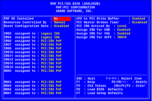
An early Plug & Play BIOS Screen
If you're using Windows 95 or later, set "PNP OS Installed" to "Yes". Unless you have any problems with your devices, that's all you need to do. If you're only using DOS, you want to set "PNP OS Installed" to "No". When this is done, you can force an IRQ (Interrupt Request Line) to be reserved for use by your non-PnP ISA card(s) by setting that IRQ to "Legacy ISA". IRQs are basically communication lines that devices can use to talk directly to the CPU and ask for some time to process something. By setting one of these to "Legacy ISA" you are effectively telling Windows to *not* assign anything automatically to that IRQ, so your non-PnP card can be jumpered to work on that IRQ.
When IBM first created their model 5150, they pre-allocated IRQ lines to certain uses. Here's a list of the most common uses of IRQs in DOS:
| IRQ | Device/Use | Notes |
|---|---|---|
| 0 | System timer | Not changeable. |
| 1 | Keyboard controller | Never available to other devices. |
| 2 | Tied to IRQs 8-15 | Some older EGA cards use this. |
| 3 | COM2 (2nd Serial port) | |
| 4 | COM1 (1st Serial port) | |
| 5 | Sound card or LPT2 (2nd Parallel port) | If you've disabled your parallel ports elsewhere in the BIOS, this will free up IRQ5 and IRQ7 for other devices. |
| 6 | Floppy disk controller | Rarely an option to be used by something else, as most systems have a FDC (Floppy disk controller). |
| 7 | Sound card or LPT1 (1st Parallel port) | If you've disabled your parallel ports elsewhere in the BIOS, this will free up IRQ5 and IRQ7 for other devices. |
| 8 | Realtime clock | Never available to other devices. |
| 9 | Substitute for IRQ2 | Sometimes used by network cards. Also used by IRQ2 to talk to the CPU - it has a higher priority, system-wise, over other IRQs. |
| 10 | (free) | Sometimes used by network cards or SCSI host adapters. |
| 11 | (free) | |
| 12 | (free) | |
| 13 | Math co-processor | Free if you don't have a math co-processor. |
| 14 | PS/2 mouse or Primary hard disk controller | |
| 15 | Secondary hard disk controller |
Some ISA cards are actually hardwired to a specific IRQ. For example, the Roland MPU-401 interface is hardwired to use IRQs 2 and 9. If you happen to have another device that also can only work on those IRQs you will have a conflict, and those two devices simply won't work together on the same PC. Fortunately, most expansion cards and devices have the ability to work on 2 or 3 different IRQs. For example, the Creative Labs Sound Blaster cards can usually be assigned to IRQ3, IRQ5 or IRQ7. Most devices only need to be assigned to a single IRQ and many don't even need an IRQ assignment at all !
Other Settings Found on Older BIOS
On 386 and 486 motherboards, you will often come across these settings.
Hard Disk Type 47 RAM Area
Extended ROM RAM Area
Extended BIOS RAM Area
Scratch RAM Option
These options configure how the BIOS scratch area in RAM is accessed. The scratch area is used to store the details of the "USER" hard disk settings (Type 47), if indeed you've chosen that type of hard disk. Older motherboards will just have a '1' or '0' for this setting (1 meaning enabled, which will use 1 KB of RAM for this storage, and 0 meaning disabled - I'm not sure what the significance is if you choose type 47, enter in the details and then choose '0' here). Newer motherboards usually give you two options:
*
“DOS 1 KB” which reduces the 640 KB conventional memory to 639 KB and it uses this 1 KB area to access scratch area;
*
“0:300” that uses address 300h to access this scratch area. The first option is preferable as the second option can frequently cause a conflict with sound cards which default their MIDI port to this address. Also network cards often use this port address to communicate with the processor.
Clock Sources Selected
Processor Clock - Processor Oscillator
CPU Clock Source - CLK2IN, CLKIN/8 or CLKIN/6
Before the days of Front Side Bus and CPU clock multipliers, we had clock sources. Motherboard chipsets usually have a dedicated "bus controller" chip, part of whose job it is to provide clock generation for the rest of the board (think of it as setting a regular pulse for different bits of the hardware). On older chipsets the bus controller has 2 clock inputs: CLK2IN and ATCLK. Typically ATCLK should be lower frequency than CLK2IN. The bus controller generates a processor clock called PROCCLK and another clock for the AT bus called SYSCLK (or SCLK).
PROCCLK can be derived from CLK2IN or from ATCLK. Under normal operation this would be set to CLK2IN to allow the processor to run at full speed.
Bus Speed Select - CL2KIN/2, CLK2IN/3
Bus Clock - PROC CLOCK/3
Just as above with the CPU Clock Source, older motherboards allowed you to select how fast you wanted the motherboard to run. You typically want to run the motherboard at the fastest speed you can, but the AT bus is very slow (8 MHz). To overcome this problem, the chipset's bus controller provides two state machines - one for the CPU which runs off CLK2IN, and the AT bus state machine which runs off BCLK. This gives the option of dividing the main crystal oscillator by a certain number, e.g. "clock input divided by 2" or "clock input divided by 3". Of course the lower the number, the faster the bus would be but you risk stability problems (hangs, system reboots, etc) as many ISA expansion cards cannot be run faster than 8 MHz. There is also SYSCLK which is the AT system clock, and is always set to BCLK/2. In normal circumstances, BLCK is half the CLK2IN (so you'll see it as CLK2IN/2) and SYSCLK is CLK2IN/4. With these settings you have the following:
I/O cycles have 1 delay, 8-bit AT memory cycles have 4 wait states, 16-bit memory cycles have 1 wait state. Alternatively, you can set BCLK to be CLK2IN, which runs the AT bus state machine at the same frequency as the CPU If the CPU is set to CLK2IN also). Setting the AT bus clock only impacts ISA cards, not VESA Local Bus cards, because the latter run at CPU bus clock speeds (25 MHz, 33 MHz, etc).
If you change the crystal oscillator used by the CPU, take not that you're also changing the AT bus speed, so you must use this setting to compensate and keep the AT bus running nice and slow (8 MHz typically, possibly going up to 12 MHz as a maximum if your expansion cards allow).
DMA Clock - SCLK/2
Just as above with the CPU and Bus Clock Sources, older motherboards allowed you to select how fast you wanted the DMA controller to run as well. The bus controller (part of the chipset) controls all bus activity and provides arbitration between the CPU, DMA and memory.
Fast Gate A20 Option
A20 (Addressing Line 20) refers to the first 64 KB of extended memory
(A0 to A19) known as the "high memory area".
This option uses the fast gate A20 line, supported
in some chipsets, to access memory above 1 MB. Intel 8088/8086 and 80186 processors only got address lines A0 through A19 as they were limited to only accessing the first 1 MB of RAM, so you won't see this option on those motherboards.
Normally all RAM access above 1 MB (specifically the A20GATE and CPU Reset (RC) are controlled by the Intel 8042 keyboard controller chip to switch the CPU between the real and protected address modes and to warm-boot the system. The operation of the 8042 is slow. Using this
option will make the access faster than the normal
method because your chipset will emulate an 8042 - one that is much faster. This feature is completely transparent to software, and is very useful in networking
operating systems.
Hidden Refresh
Allows the RAM refresh memory cycles to take place
in memory banks not used by your CPU at this time,
instead or together with the normal refresh cycles,
which are executed every time a certain interrupt
(DRQ0 every 15 msecs) is called by a certain timer
(OUT1). Every time it takes 2 to 4 msecs for the
refresh. One refresh cycle every ~16 us refreshes 256
rows in ~ 4ms. Each refresh cycle only takes the
equivalent of one memory read or less, as CAS
(Column Address Strobe) is not needed for a refresh
cycle. Some RAMs can do it, some not. Try. If the
computer fails, turn it off. Enabled recommended.
There are typically 3 types of refresh schemes: cycle steal,
cycle stretch, or hidden refresh. Cycle steal actually steals
a clock cycle from the CPU to do the refresh. Cycle
stretch actually delays a cycle from the processor to do
the refresh. Since it only occurs every say 4ms or so, it's
an improvement from cycle steal. We're not really
stealing a cycle, only stretching one. Hidden refresh
typically doesn't stretch or steal anything. It's usually tied
to DTACK (Data acknowledge) or ALE (Address Latch
Enable) or some other signal relating to memory access.
Since memory is accessed ALL of the time, ie ram, rom,
etc. it's easy to synchronize the the refresh on the falling
edge of this event. Of course, the system performance is
at its optimum efficiency, refresh wise sinces we're not
taking clock cycles away from the CPU.
Slow Refresh
Causes RAM refresh to happen less often than usual.
This increases the performance slightly due to the
reduced contention between the CPU and refresh
circuitry, but not all DRAMs necessarily support these
reduced refresh rates (in which case you will get parity
errors and crashes).
Concurrent Refresh
Both the processor and the refresh hardware
have acces to the memory at the same time. If
you switch this off, the processor has to wait until
the refresh hardware has finished (it's a lot
slower). Enabled recommended.
Single ALE Enable
ALE (Address Latch Enable) is a pin on your
PC-bus that is active each time there is an address
on the bus. May slow the video bus speed is
enabled. Still very obscure.
Fast Decode Enable
Refers to some hardware that monitors the commands sent
to the keyboard controller chip. The original AT used special
codes not processed by the keyboard itself to control the
switching of the 286 processor back from protected mode to
real mode. The 286 had no hardware to do this, so they
actually have to reset the CPU to switch back. This was not
a speedy operation in the original AT, since IBM never
expected that an OS might need to jump back and forth
between real and protected modes. Clone makers added a few
PLD chips to monitor the commands sent to the keyboard
controller chip, and when the "reset CPU" code was seen, the
PLD chips did an immediate reset, rather than waiting for the
keyboard controller chip to poll its input, recognize the reset
code, and then shut down the CPU for a short period. This"fast decode" of the keyboard reset command allowed OS/2
and Windows to switch between real and protected mode
faster, and gave much better performance. (early 286 clones
with Phoenix 286 BIOS had this setting to enable/disable the
fast decode logic.) On 386 and newer processors, the fast
decode is probably not used, since these CPUs have hardware
instructions for switching between modes. There is another
possible definition of the "Fast Decode Enable" command.
The design of the original AT bus made it very difficult to mix
8-bit and 16-bit RAM or ROM within the same 128K block of
high address space. Thus, an 8-bit BIOS ROM on a VGA
card forced all other peripherals using the C000-Dfff range to
also use 8 bits. By doing an "early decode" of the high
address lines along with the 8/16 bit select flag, the I/O bus
could then use mixed 8 and 16 bit peripherals. It is possible
that on later systems, this BIOS flag controls the "fast decode" on these address lines.
Extended I/O Decode
The normal range of I/O addresses is 0-0x3ff;
10 bits of I/O address space. Extended
I/O-decode enables wider I/O-address bus. The
CPU(s) support a 64K I/O space, 16 address
lines. Most motherboards or I/O adapters can be
decoded only by 10 address bits.
I/O Recovery Time
When enabled, more I/O wait states are
inserted. A transfer from IDE harddrive to
memory happens without any handshaking,
meaning the data has to be present (in the cache
of the harddisk) when the CPU wants to read
them from an I/O Port. This is called PIO
(Programmed I/O) and works with a REP INSW
assembler instruction. Now I/O Recovery Time
enabled adds some wait states to this instruction.
When disabled, the harddrive is a lot faster. Note
that there is a connection between I/O Recovery
Time and AT BUS Clock Selection. For
example, if the AT BUS Clock is set to 8 MHZ
and you have a normal harddisk, I/O Recovery
Time can be turned off, resulting in a higher
transfer rate from hard disk.
Memory Read
Wait State
Wait states are used for RAM which isn't fast enough for
the computer. On a 486, 1 or more wait states are often
required for RAM with 80ns or higher access times.
And, depending on the processor and motherboard, also
for lower than 80ns access times. The fewer the wait states,
the better. Consult your manual. If wait states are too
low, a parity error will occur.
For 386 or 486 non-burst memory access cycle takes 2 clock ticks. A *rough* indication of RAM speed necessary for 0 wait states is 2000/Clock[MHz] - 10 [ns]. For a 33Mhz processor, this would give 50ns of access time required. The number of wait states necessary is *approximately* (RamSpeed[ns] +10) * Clock[MHz] /1000 - 2. For 70ns RAM and a 33Mhz processor (very standard configuration), this would give roughly 1 wait state. But this really is dependent on chipset, motherboard and cache design, CPU type and whether we talk about reads or writes. Take these formulas with a large grain of salt. You can find out the access time of your RAM chips by looking at their product numbers. Mostly at the end there is a 70, 80, 90, or even 60. If 10 stands there, it means 100 ns. Some RAM chips also have an explicitly written speed in ns. The RAM you buy these days mostly have 70ns or 60ns.
Memory Write Wait State
(as above)
Cache Read Option
Often also called "SRAM Read wait state", (SRAM:
Static Random Access Memory) taking simple
integer values, or "SRAM Burst", with options like 2-1-1-1,
3-1-1-1 or 3-2-2-2. This determines the number
of wait states for the cache RAM in normal and
burst transfers (the latter for 486 only). The
lower the series of numbers your computer can support, the better, so 2-1-1-1 will be faster than 3-1-1-1.
Cache Write Option
Same thing as memory wait states, but refers to your motherboard's cache ram, not main memory.
Non-Cacheable
Block-1 Size
Disabled. The Non-Cacheable region is intended for
a memory-mapped I/O device that isn't supposed to be
cached. For example, some video cards can present all
video memory at 15 meg - 16 meg so software doesn't
have to bank-switch. If the non-cacheable region covers
actual RAM memory you are using, expect a significant
performance decrease for accesses to that area. If the
non-cacheable region covers only non-existent memory
addresses, don't worry about it. If you dont want to
cache some memory you can exclude 2 regions of
memory. There are *good* reasons not to cache some
memory areas. For example, if the memory area
corresponds to some kind of buffer memory on a card
so that the card may alter the contents of this buffer
without warning the cache to invalidate the
corresponding cache lines. Some BIOSes take more
options than enabled/disabled, namely Nonlocal/Noncache/Disabled (VLB only?).
Non-Cacheable Block-1 Base
0KB. Enter the base address of the
area you don't want to cache.
Cacheable RAM
Address Range
Usually chipsets allow memory to be cached just up to
16 or 32 MB. This is to limit the number of bits of a
memory address that need to be saved in the cache
together with its contents. If you only have 4 MB of
RAM, select 4 MB here. The lower the better, don't
enter 16MB if you only have 8 MB installed!
Video ROM Shadow C000,16K
Memory hidden under the "I/O hole" from 0x0A0000
to 0x0FFFFF may be used to "shadow" [copy] code in your video ROM (Read-Only Memory) chip. By doing so, the contents of the ROM are
copied into the RAM and the RAM version is used instead.
Video BIOS is stored in slow EPROM (Erasable
Programmable Read-Only Memory) chips (120 to 150ns
of access time). Also, ROM is 8- or 16-bits while RAM
is 32-bit-wide access. With ROM Shadow on, the EPROM
content is copied to RAM (60 to 80ns of access time
with 32-bit-wide access). Therefore perfomance
increases significantly. Only sensible on EGA/VGA
systems. Enabled recommended.
If you have flash
BIOS, you can disable it. Flash BIOS enables access at
speeds similar to RAM memory access so you can use the
memory elsewhere. However, flash BIOS is still only
accessing it at the speed of the bus (ISA, EISA or
VLB). On systems where the BIOS automatically steals
384k of RAM anyway, it shouldn't hurt to enable
shadowing even on flash ROM. One side effect is that
you will not be able to modify the contents of flash
ROM when the chip is shadowed. If you reconfigure an
adapter which you think might have flash ROM, and
your changes are ignored, or of course if it gives you an
error message when you try to change them, you'll need
to temporarily disable shadowing that adapter. On
(S)VGA you should enable both video shadows. Some
video cards maybe using different addresses than C000
and C400. If it is the case, you should use supplied
utilities that will shadow the video BIOS, in which case
you should disable this setting in the CMOS. Video
BIOS shadowing can cause software like XFree86 (the
free X Window System) to hang. They should be
probably be disabled if you run any of the 386 Unix flavours.
Adaptor ROM Shadow
C800,16K
Disabled. Those addresses (C800 to EC00) are
for special cards, e.g. network and controllers.
Enable only if you've got an adapter card with
ROM in one of these areas. It is a BAD idea to
use shadow RAM for memory areas that aren't
really ROM, e.g. network card buffers and other
memory-mapped devices. This may interfere
with the card's operation. To intelligently set
these options you need to know what cards use
what addresses. Most secondary display cards
(like MDA and Hercules) use the ROM C800
address. Since they are slow, shadowing this
address would improve their performance. An
advanced tip: in some setups it is possible to
enable shadow RAM *without* write-protecting
it; with a small driver (UMM) it is then possible
to use this 'shadow RAM' as UMB (Upper
Memory Block) space. This has speed advantages
over UMB space provided by EMM386.
System ROM Shadow F000,64K
Same thing as Video shadow, but
according to the system bios (main
computer BIOS). Enabled
recommended for improved
performance. System BIOS
shadowing and caching should be
disabled to run anything but MS-DOS. NOTE: On some BIOS versions (probably newer ones) the shadow
choices are in 800(hex)-byte increments. For instance, instead of two
Video ROM Shadow segments of 16K (C400 and C800), you will have
one 32K segment. Same thing for Adaptor ROM Shadow segments.
Dumping the BIOS ROM
Motherboard manufacturers will often release updated firmware as new CPUs become available or they need to patch a bug found in the code. The process of updating your BIOS version is known as "flashing" or "burning" the ROM. Usually the BIOS manufacturer provides a program alongside a new ROM file, with which you would flash your ROM to the version that's in the new ROM file.
Because upgrading / flashing your BIOS does carry some risks, it is advisable to take a backup of your existing ROM firmware (the software in the BIOS chip). If you can only get hold of an EPROM programmer and an EPROM that is larger than your original ROM, it is common practice to simply write several versions of the identical code to fill up the remaining space. For example, if your original ROM is 8KB in capacity but you only have a 16KB EPROM, just write the firmware twice.
There are various DOS utilities that can assist in dumping your current BIOS firmware to a file. See the Downloads page for these.