Motherboards
Motherboards up to and including the 80386 era usually had their CPU socketed, but it was rare to swap out the CPU for a faster one. Starting with the i486 era around 1990, motherboards began to support a broader range of CPUs and speeds, which allowed owners to upgrade their CPU without necessarily having to also upgrade other components including the motherboard.
This page describes the various motherboards, and their socket / slot types. For pre-Socket 3 motherboard info, there are a few pages at DOS Days that may have what you're looking for. Try XT motherboards, 286 motherboards, or 386 motherboards. For a [fairly] comprehensive list of all motherboards on DOS Days, check out the main Hardware page and choose a manufacturer.
Socket 3 (1990-1992)
Sockets 1 and 2 were never formally released, so starting with Socket 3, these were for Intel 80486DX / 486SX / 486 Overdrive / 486DX2 / 486DX4, AMD 5x86, and Cyrix 5x86 CPUs.
Socket 3 was created because Intel dropped the voltage of their CPUs from 5V down to 3.3V. Socket 3 permitted the new 3.3V CPUs - these new CPUs were designed to deliberately *not* fit into an older 5V socket due the rearrangement of the pin layout. Socket 3 has 237 pins and takes PPGA (Plastic Pin Grid Array) chips.
Socket 3 motherboards usually support both 5V and 3.3V CPUs ranging in speed from 25 MHz up to 50 MHz. During the Socket 3 era, CPU heatsinks and fans (often abbreviated to "HSF") started to become necessary with some of the faster CPUs to prevent overheating. These days I always fit a heatsink and/or fan to 486s if the clock speed is 50 MHz or higher.
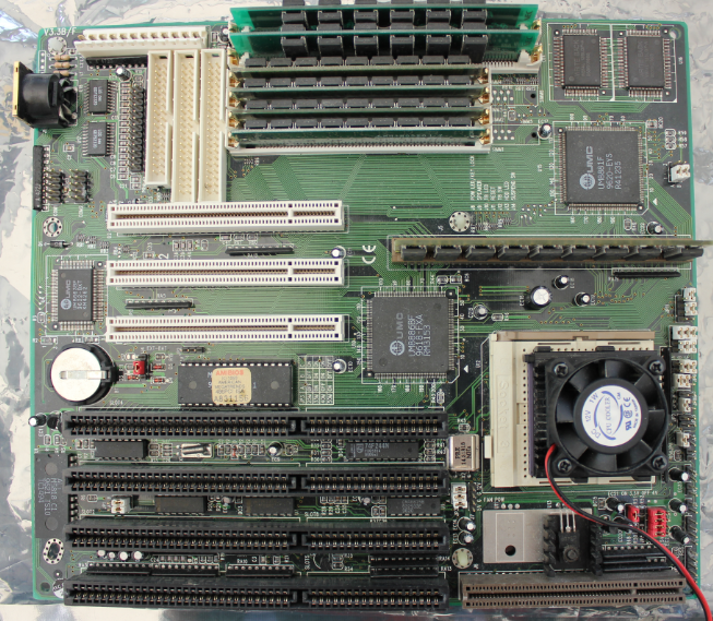
A PC Chips M919 Socket 3 motherboard from 1993
Socket 5 (1993-1997)
Socket 5 was created for the 2nd generation of Pentium processors (called "P54C"), with CPU speeds ranging from 75 MHz up to 120 MHz. It also supported Pentium MMX and Pentium OverDrive processors. All CPUs for Socket 5 ran with a 3.3V core voltage. The pin arrangement on the socket (and associated CPU) were staggered which allow the pins to be closer together. Socket 5 has 320 pins and takes SPGA (Staggered Pin Grid Array) chips.
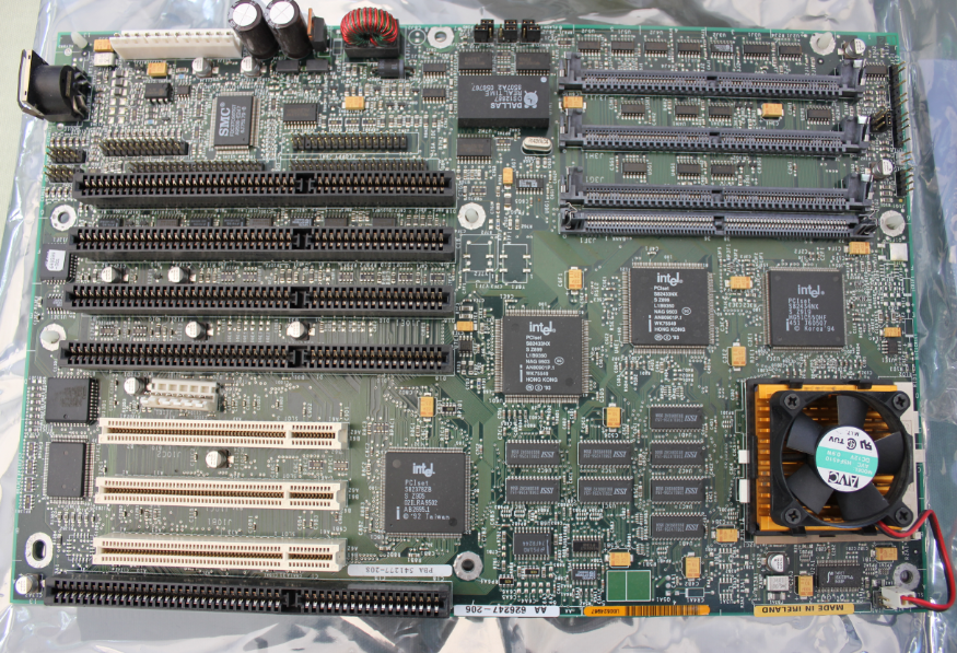
An Intel Premiere PCI Plato II Socket 5 motherboard
from 1994
Socket 7 (1995-1999)
Socket 7 is renowned for being probably the most flexible socket in terms of the number of different CPUs and range of clock speeds it can support. It was widely adopted by Intel, AMD, Cyrix and ITT among others.
Socket 7 supports P5 Pentium and Pentium MMX, AMD K5 and K6, Cyrix 6x86 and 6x86MX, IDT WinChip, and more. It is also favoured by retro computing enthusiasts today because it was during this time that a separation took place between the clock speed of the CPU, and that of the bus - referred to as the Front Side Bus (FSB), allowing hardware and other devices to no longer be restricted by the CPU's bus clock.
A Socket 5 CPU can be placed in a Socket 7 motherboard - Socket 7 is backwards compatible.
Super Socket 7 (1997)
Not so much a new socket, but an extension to the Socket 7 standard, Super Socket 7 (officially called "Super7") was developed by AMD to support their new K6-2 and K6-III processors.
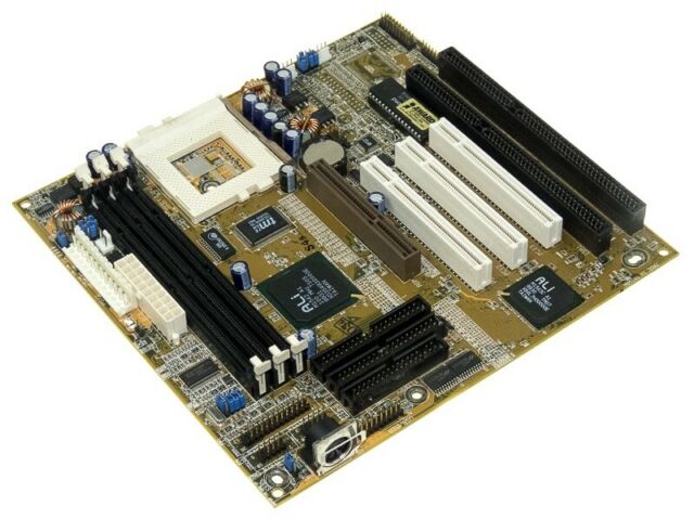
The ASUS P5A Super Socket 7 motherboard
It overcame a number of limitations that the earlier Socket 7 specification had. With Super Socket 7 came the ability to increase the bus clock speed (Front Side Bus) from 66 MHz to 100 MHz, which brought significant performance improvements for all systems using this new socket, helping it keep pace with its Intel rival with their Pentium II and its Slot 1 architecture. It also added support for PC100 SDRAM memory as well as AGP (Advanced Graphics Processor) 2x graphics.
There is no visual difference between a Socket 7 and a Super 7 motherboard (aside from perhaps the presence of an AGP slot) - they have an identical 321-pin grid array (PGA) 'Socket 7' socket for the CPU so you will need to check the board's chipset to confirm if it supports the 100 MHz FSB speed of Super 7, or the slower 66 MHz FSB speed of Socket 7.
Super Socket 7 typically will cater for all Socket 7 processors, but also supports the higher clock rates of the faster AMD chips (K6, K6-2, K6-III and their '+' variants). In some cases, Super Socket 7 motherboards will also have explicit support for the Cyrix 6x86 and 6x86MX (MII) processor family in addition to the AMD CPUs.
For more information, see also my comparison page of Socket 7 vs Super Socket 7.
Slot 1 (1997)
When Intel launched the Pentium II CPU in 1998, they did so alongside their new "Slot 1" motherboard interface. Slot 1 replaced the short-lived Socket 8 for the Pentium Pro where they had combined the processor and cache dies into a single package. This was uneconomical, as they had to be bonded very early in the manufacturing process, so any flaws that were detected in one (a quite common occurrence) was costly, as the entire package had to be discarded. Their answer was to mount both dies onto a card (a "Single Edged Contact Cartridge, or SECC). Because these were on the same card meant they were closely-coupled enough for high performance, whilst reducing wastage due to faulty dies.
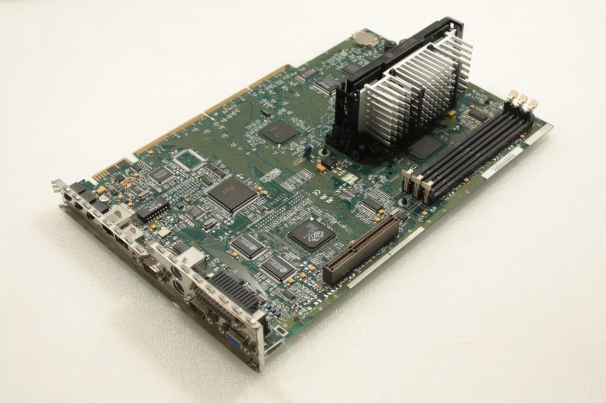
A Compaq motherboard with a Pentium II installed in its Slot 1 slot
Initially, the first Pentium II CPU, "Klamath", was seen on Slot 1 boards alongside Intel's 440FX chipset (also used with the earlier Pentium Pro). Then the 440LX chipset which added AGP 2x support as well as SMP (Symmetric Multiprocessing, basically two Slot 1s on a single motherboard for parallel processing), and the cut-down 440EX with no SMP, but the game-changer was the Intel 440BX chipset which finally introduced official support for the 100 MHz Front Side Bus. The Slot 1 would continue to be used for the smaller micron manufacturing-process "Deschutes" variant (which ran on 2V instead of 2.2V of "Klamath").