Introduction
At the heart of a PC is the bus. In essence, this permits the CPU to access main memory and other peripherals, including expansion cards.
ISA (1982-2002)
ISA is a bus architecture used in all PCs and their compatibles from 1982 through to the early 2000s. The ISA, or Industry-Standard Architecture, bus began life with the IBM 5150, their first PC. Back then it was simply called the PC bus and later called the AT bus after IBM launched the 5150's successor, the 5170 PC/AT, with its introduction of 16-bit expansion slots.
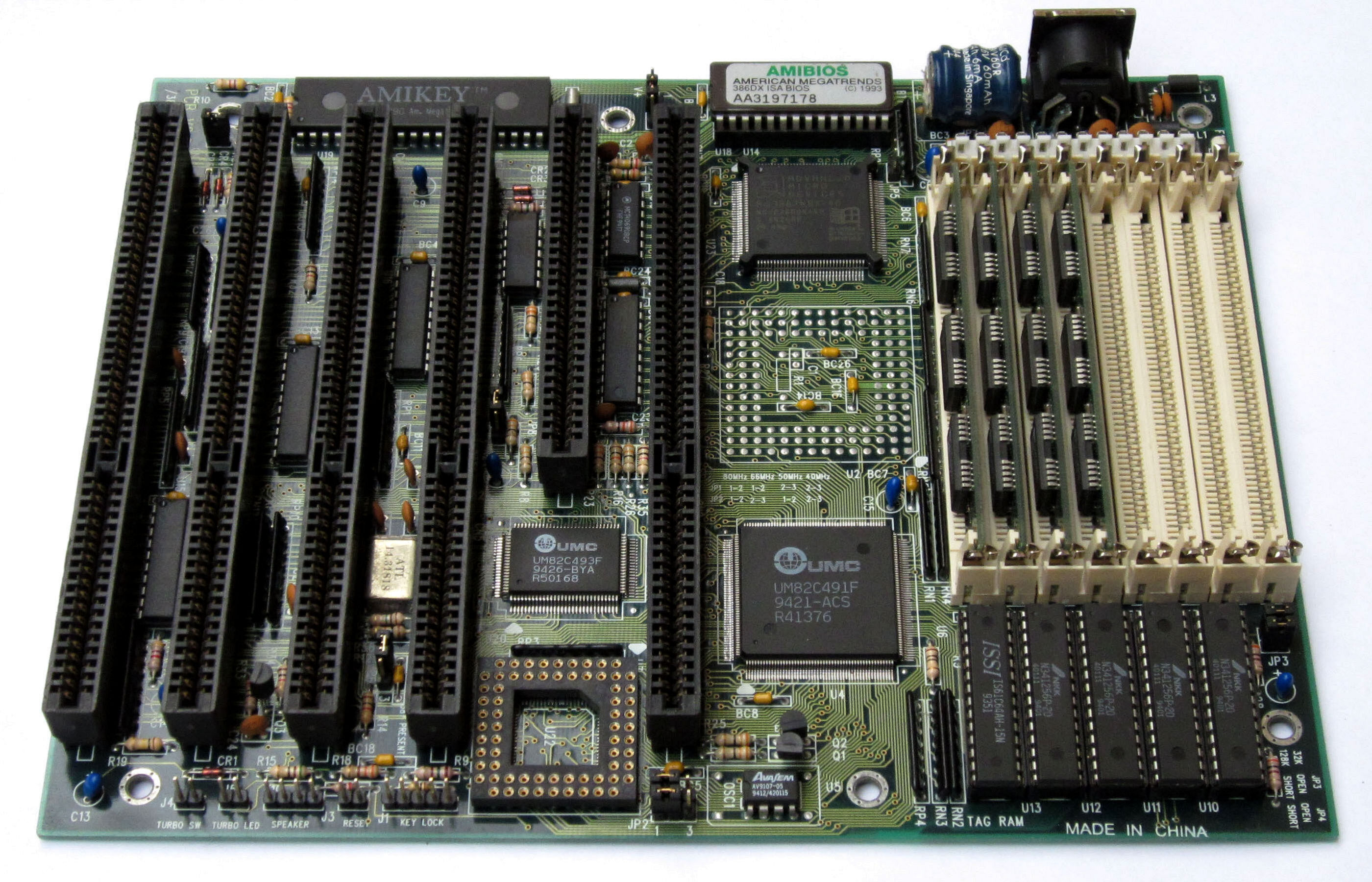
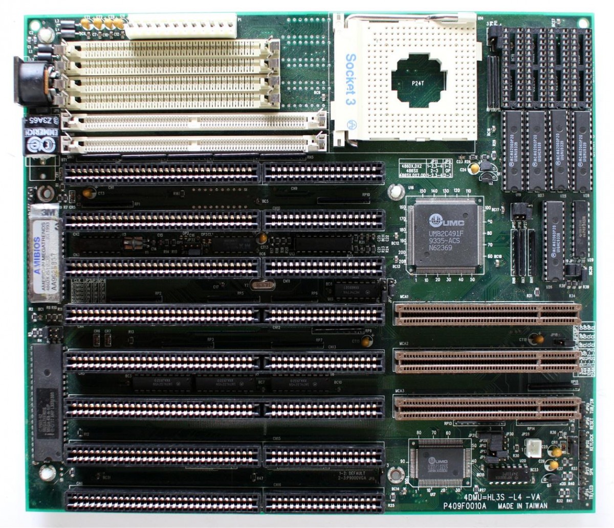
A 386 motherboard with one 8-bit and five 16-bit ISA slots
The first IBM PC and XT ran an Intel 8088 which was 16-bit CPU internally, but communicated with the outside world at 8-bits. This meant the motherboard on the IBM PC and IBM XT were both 8-bit, so the PC bus (as ISA was called back then) was also 8-bit.
With the introduction of the IBM AT in 1984, the new Intel 80286 had a 16-bit data width, so the CPU and motherboard could communicate together at twice the performance. To ensure peripheral cards also got the benefit of this faster bus speed, the AT bus was created as a backward-compatible extension of the PC bus, and allowed for 16-bit communication.
The ISA bus is an 8-bit or 16-bit communication highway that originally ran at the same clock speed as the CPU. In the original IBM PC and XT, they used the same crystal oscillator as the CPU, so both CPU and bus ran at 4.77 MHz. With the arrival of the IBM 5170 AT, it still shared a crystal oscillator with the CPU, so the bus and CPU both ran at 6 MHz in the early models, and later at 8 MHz. This simple synchronous design avoided technical headaches with timings between peripheral cards and the main computer. IBM never published actual timings for the ISA bus, so clone manufacturers used IBM's circuit diagrams to develop approximate timing rules. As clock speeds rose, these approximations didn't work so well beyond the rough 8 MHz bus speed. Due to the slowness of the bus and the I/O bottleneck that it caused, both IBM and others looked for ways to increase bus speeds. The ISA bus could actually run at up to 16 MHz, using the I/O Channel Ready line to receive the signal from the bus that it is available for another instruction, but this was rarely implemented as nobody could agree on exactly when to use it.
As PCs became faster around the ISA bus, maximum bandwidth was realised at around 6 Mbps (megabits per second), compared to 132 Mbps on the later PCI bus.
Micro-Channel Architecture
MCA, or Micro-Channel Architecture was IBM's attempt in 1987 to regain control of the PC market, which was awash with competitors manufacturing and selling their own 'IBM-compatible' computers. Recognising the 8 MHz limitations of the ISA bus, and in-line with them introducing their new PS/2 range of PCs they also introduced the world to their new higher-speed expansion bus, MCA.
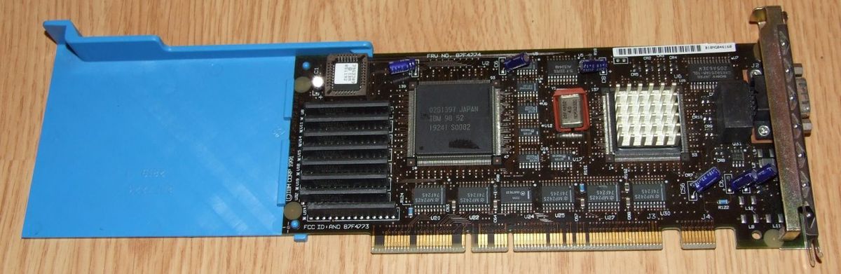
An IBM XGA Graphics Card from 1987
IBM of course really wanted to control the expansion card market as well as the computer market as a whole. The plan was to allow only licenced 3rd-party peripheral companies to create and sell expansion cards that worked on the faster Micro-Channel bus. Some of the larger 3rd-parties did pay IBM for an MCA licence and manufactured their cards to work on the new bus, but IBM's licence costs were astronomical, which resulted in MCA being rather shortlived, with most IBM-compatible vendors choosing to stick to the traditional 'AT' bus (as it was originally known, later commonly referred to as the ISA bus).
Technically, MCA was streets ahead. It ran a 32-bit wide data bus and had a dedicated bus controller which was able to do "burst mode" transfers. Even at its introductory speed of 10 MHz, it was five times faster than the AT bus, able to perform up to 40 MB/second throughput.
One downside to MCA was lack of backward-compatibility - there wasn't any kind of "bridge" between ISA and MCA for users wanting to move gradually to the new 32-bit standard.
EISA
After PC-compatibles started arriving on the scene, in 1987 a group of nine competing PC manufacturers called the "Gang of Nine" designed a new 32-bit bus called EISA, or Extended Industry Standard Architecture. Members of the consortium were Compaq, AST, Epson, Hewlett-Packard, NEC, Tandy, Wyse, Zenith and Olivetti. In 1987, this group held a 33.5% market share of the PC market (28.8% in 80286s and 43.1% in 80386 PCs). By comparison, IBM's market share had dropped to 26.8% (28% of the 80286 market and 16.1% of the 80386 market). The rest was made up of other non-"Gang of Nine" PC manufacturers. It was the 386 market the Gang of Nine were aiming for, as this was where increased bus performance really mattered, and where IBM's Micro-Channel Architecture bus and the EISA bus would compete head-to-head.
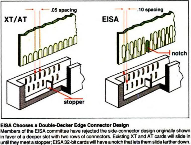
By January 1989, they had agreed upon the new bus connector which used a "double-decker" edge connector design (see picture). To avoid infringing on IBM's trademark "AT Bus", they renamed the original bus "ISA" (since it wasn't "extended"). EISA was 100% backward-compatible with the ISA bus having the same length and width as existing PC AT connectors, but EISA was deeper, so a standard ISA card would work when put in an EISA slot, stopping when they hit a 'stopper' half-way into the deeper slot. EISA cards would go down further and connect with a second row of contacts.
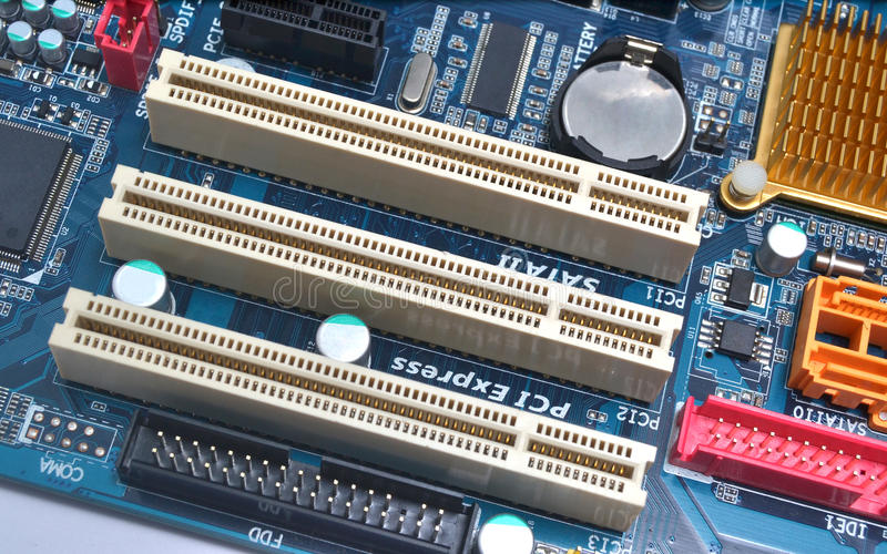
The EISA bus was a further extension of the AT bus from 16 bits to 32 bits. Bus mastering support was extended to now be able to address up to 4 GB of main memory, and it also supported bus sharing between multiple CPUs. EISA slots were typically brown to distinguish them from 16-bit ISA slots which were usually black (the motherboard below is an exception, as it has brown ISA slots as well).
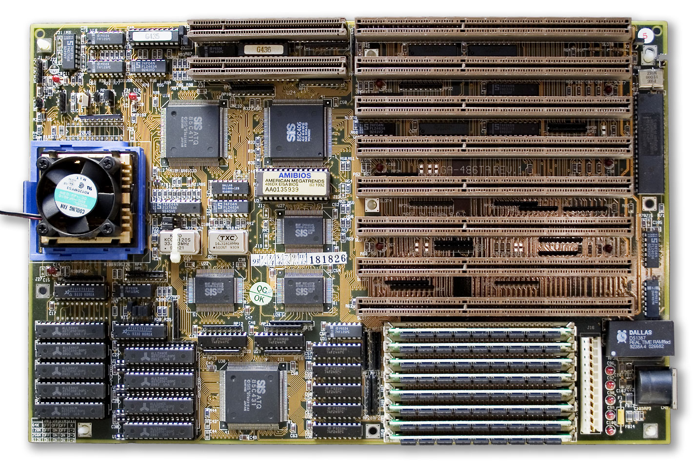
A 486DX motherboard with two 32-bit EISA slots and six 16-bit ISA slots
Compatibility
All ISA/EISA cards are backward-compatible, meaning if you have an 8-bit ISA expansion card, it will work in an 8-bit or 16-bit ISA slot, or the rearmost part of an EISA slot. Likewise, a 16-bit ISA expansion card will work in a 16-bit ISA slot or in an EISA slot, but not typically in an 8-bit slot.
In some rare cases there is forward-compatibility - a 16-bit ISA card is designed to work in an 8-bit or 16-bit slot. Such cards sometimes have a jumper to set which tells the card it's running in an 8-bit slot. This is especially true of early 16-bit graphics cards.
PCI (1992-2004)
The Peripheral Component Interconnect (PCI) bus was introduced in 1992 as a standardised replacement for the aging ISA bus, which was by now extremely slow and hence was the primary cause of performance bottlenecks in PCs. PCI was first seen on servers, replacing MCA and EISA as the bus of choice for faster throughput (up to 132 Mbps bandwidth).
A motherboard with three PCI slots
The first version of PCI (v1.0) was a 32-bit bus and used a 33 MHz bus clock with 5V signalling*. This provided a throughput of up to 133 MB/s. Version 2.0 of the PCI standard introduced 3.3V cards and these were physically different, having the notch at the other end. Universal PCI cards have both notches, and can be used either in PCI v1.0 and PCI v2.0 slots. With the introduction of PCI v2.1, 66 MHz bus speeds were achievable, so throughput was now up to 266 MB/s for 32-bit cards or 533 MB/s for 64-bit cards (these are quite rare in the consumer market - it's highly likely all your PCI cards are 32-bit).
PCI was slower to replace the VESA Local Bus, not seeing widespread adoption until 1994, during the era of the second-generation Pentium CPUs. By 1995, VLB was gone, with motherboard manufacturers having moved fully to PCI, even for 486 computers.
*This lack of a 3.3V line on the PCI v1.0 bus means it is likely you will have issues with later [v2.2+] PCI cards that require 3.3V. One tell-tale that your motherboard is an early PCI one is the presence of both an AT and ATX power connector.
VESA Local Bus (1992-1994)
The VLB standard, as its often abbreviated, was created by the Video Electronics Standards Association (VESA) in Autumn 1992 in order to provide a much faster bus for graphics cards to access main memory. The traditional ISA bus up to this point had made sense - there was no need to improve performance of slower-running peripheral boards that could not transfer enough data to saturate the expansion bus. But the data traffic of some peripherals - particularly graphics cards at this time - had outgrown what the standard 16-bit 8 MHz ISA expansion would bear.
This bus was a little different in that standard low-speed operations could still use the ISA bus on which it sat whilst using its own faster conduit for DMA (Direct Memory Access) transfers and memory-mapped I/O. This would run at the same speed as the CPU, so if you were running a VLB graphics card on a 486DX-33 you could expect four times the data throughput compared to the same operation using an ISA graphics card (33 MHz compared to 8 MHz). One of the first graphics chipsets to make use of the VESA Local Bus was S3's 86C805, which was essentially the same as their 86C801 ISA chipset, but with the addition of a 32-bit I/O interface for the local bus.
The idea of a "local bus" didn't start with VESA. Numerous motherboard manufacturers were already creating their own local buses on their boards, and up to mid-1992 no VESA standard had yet been enacted. Because of this, early boards with a local bus required the owner to also purchase local bus expansion cards from the same manufacturer as the mainboard, in order to be compatible.
The VLB standard was designed as a stop-gap to alleviate performance bottlenecks on 486 systems when running graphical user interfaces and other graphically-intensive software (games). In order to achieve widespread adoption by motherboard manufacturers, the design was supposed to be simple to implement and cost-effective.
A 486 motherboard with eight 16-bit ISA slots, of which three also support VESA Local Bus (VLB)
Unfortunately, it had a short lifespan primarily because its design was tied closely with the 486 memory bus design. With the arrival of the much-different Pentium's memory bus design, VLB was incompatible. As a result, very few Pentium motherboards come with VLB slots.
Other problems were also common when using VLB which hampered reliability. Tight electrical guidelines weren't always adhered to by card and motherboard manufacturers, and due to the fact that the bus was shared with ISA, arbitration between instructions from VLB cards and ISA cards (or simply between multiple VLB cards) could sometimes go wrong, causing memory overwrites, and possible data coruption.
As bus speeds increased towards 50 MHz, VLB became even more unreliable. This is one reason why Intel 486DX-50 didn't achieve success in the market. Its successor, the DX2-66 worked much better by adopting the slower 33 MHz FSB (Front side bus) speed, coupled with a clock multiplier of 2 (2x33 = 66 MHz).
With the move to Pentium-based PCs, VESA Local Bus died off quickly.
AGP (1997-2004)
The AGP (Advanced Graphics Processor) interface was introduced to market by Intel in Q3 1997, when Socket 7 and the first P5 Pentiums were prevalent and Intel were moving to the Slot 1 Pentium II processors.
AGP was designed to be a fast 66 MHz communications bus for the explicit use of graphics cards only. It offered up to 15 times the bandwidth of the PCI bus - from 266 Mbps (megabits per second) with AGP 1x up to 1.07 Gbps (gigabits per second) with AGP 4x.
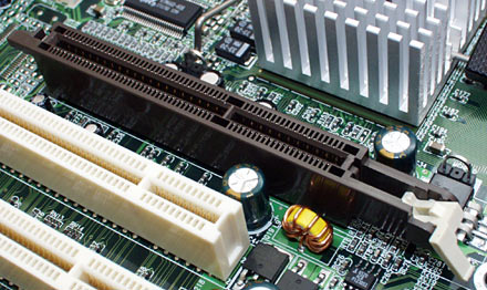
An AGP slot beside the PCI slots
There are three prime reasons for this increased bandwidth:
1) An AGP card doesn't share the bus with anyone else (like PCI cards do) - it has a direct connect to the CPU.
2) AGP cards have direct access to main memory to help with complex operations such as texturing.
3) AGP supports pipelining (multiple requests at the same time).
AGP cards can use a certain amount of main memory - the total amount available is called the AGP aperture.
Judging by the list above, you would expect an AGP card to massively outperform an equivalent PCI card running at the same internal clock frequency. In reality, AGP performance only really comes into its own at higher resolutions and in multi-texturing situations.
The first Intel chipset to support AGP was the 440LX Slot 1 chipset. Intel never made a Socket 7 chipset that supported AGP. Other chipsets that first supported AGP were VIA's Apollo VP3, SiS' 5591/5592, and ALI's Aladdin V.
The earliest graphics cards to support AGP were the Rendition Verite V2200, 3dfx Voodoo Banshee, nVidia RIVA 128, the ATi Rage series, Matrox Millennium II and S3 ViRGE GX/2.
There have been a number of versions of the AGP slot, as described below:
- AGP v1.0 - 3.3V signalling, and supports 1x and 2x speeds. Maximum bandwidth is 266 MB/s or 533 MB/s.
- AGP v2.0 - 1.5V signalling, and supports 1x, 2x and 4x speeds. Max bandwidth at 4x is 1.06 GB/s.
- AGP v3.0 - 0.8V signalling, and supports 1x, 2x, 4x and 8x speeds. Max bandwidth at 8x is 2.13 GB/s.
WARNING: Do not confuse the AGP version (1.0, 2.0 or 3.0) with the speed (1x, 2x, 4x and 8x). It's easily done if you're in a hurry and could result in permanent damage to your graphics card and/or motherboard!
To ensure incorrect voltage cards cannot be used in a slot that it's not designed for, a few 'key' slots were made on both card and slot, though not every card manufacturer adhered to this. The diagram below shows a card with a 1.5V key (AGP v2.0 standard) and a 3.3V key (AGP v1.0 standard), as well as the motherboard slots they work in.
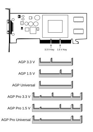
The most important thing to look for if you aren't sure if your AGP card is compatible with your motherboard, is to look up the card's operating voltage in its manual. Some cards support both 1.5V and 3.3V (in such cases only the 1.5V portion is used if supported by the motherboard). Bottom line: check both your motherboard's and your card's user manual before inserting the card and powering up.
AGP 1x ran at 66 MHz with a maximum burst data transfer rate of 264 Mbps. AGP 2x ran at 133 MHz and raised the burst rate to 528 Mbps. AGP 2x also included command pipelining and sideband addressing, which allowed for better bus utilisation.
The last graphics cards to run on AGP 1x and 2x were the ATI Radeon 8500, released in 2001, and the nVidia GeForce 3 Ti200 or Ti500. There are GeForce 4 Ti and Radeon 9250 cards that still used AGP 2x but these are very rare.
AGP 4x arrived in 1999 with the introduction of the Intel 820 chipset. This, according to Intel, doubled the transfer rate of the bus from 528 MB/sec to a whopping 1056 MB/sec.
AGP was replaced by PCI-e (PCI Express) from around 2004, although motherboards with AGP slots were still available up to 2008.