Chaintech 4SLE Motherboard - Part 1
5th July 2021
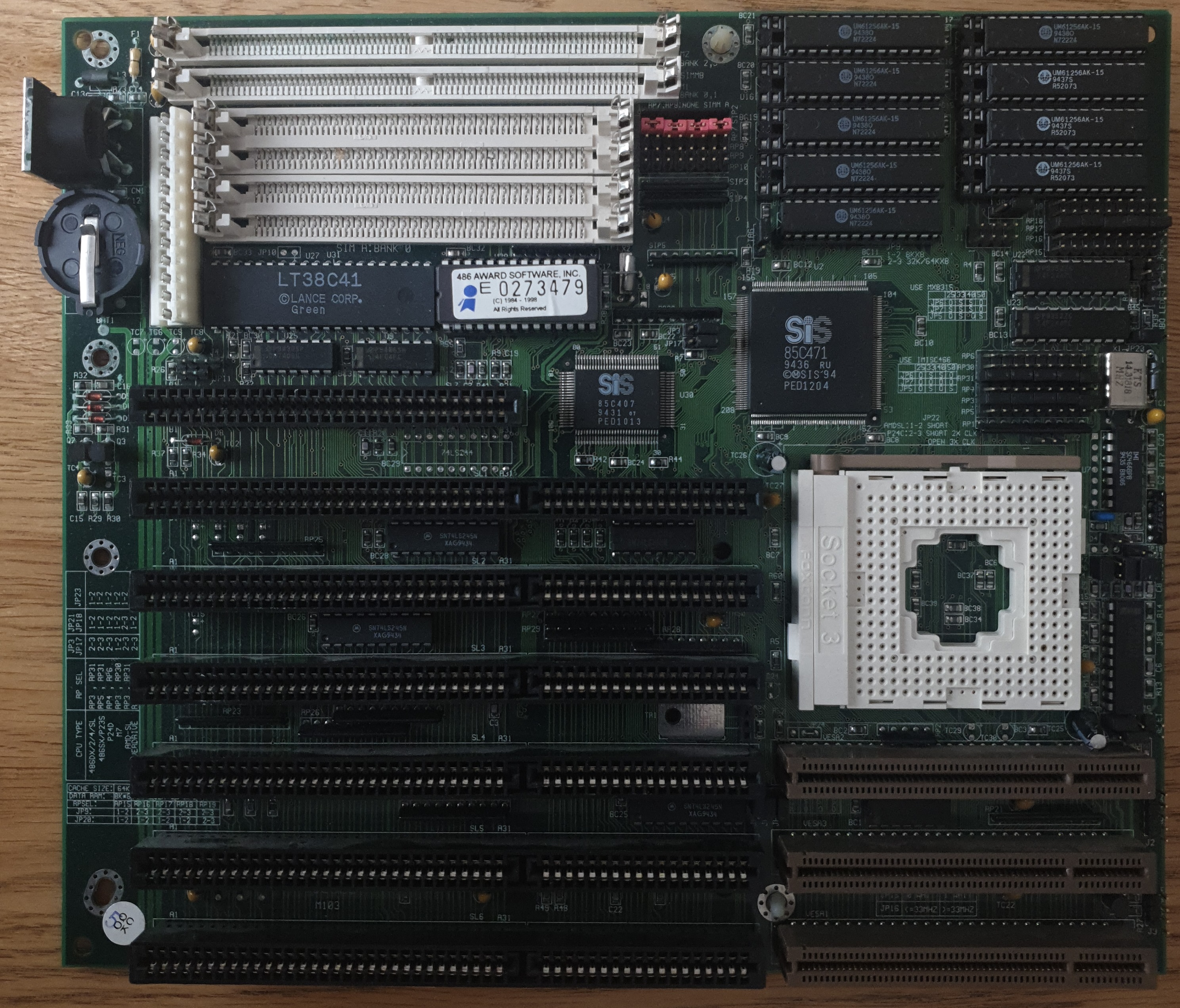
This one's been in my motherboard collection since 2011, having acquired it at auction for under £40. The Chaintech 4SLE was also sold by IPC as the "IPC Family Magic", and was the successor to their slightly earlier 4SLD.3/486SLD/486SLP which lacked 72-pin SIMM slots. Here's a quick look at this nice Baby AT board:
Quick Visual Inspection
Looking around the board it appears to comprise the following:
|
|
The board layout is ever so slightly compromised - the three non-VLB 16-bit ISA slots can only be used by short cards if you are using any CPU that requires a heatsink/fan, especially sound cards and SCSI controllers that can easily be longer than the 16-bit ISA slot. That being said, this was a common problem during the 486 era, and the fact there are three VESA Local Bus slots instead of two probably makes up for it. It also made sense to put the chipset between the CPU, cache and memory to get the best performance, so good job there, Chaintech!
Date-wise, the most recent date stamp on the motherboard's chips is week 38 of 1994, which is one of the cache chips. Most of the others have date stamps around a similar week, so these are likely originals. This date stamp puts the motherboard's manufacture around 19th September 1994, when the Pentium/Socket 5 was the new premium option, but these fast 486s with VLB were still a very cost-effective option for the masses.
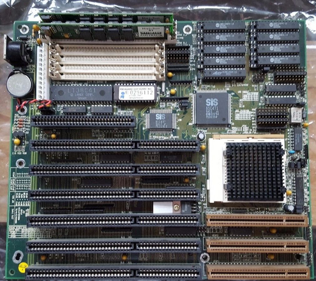
Just above the lowest ISA slot is "M103" on the silkscreen - this denotes the PCB revision. The Chaintech 4SLE is known to have had several revisions in its lifetime. Here are the ones I am aware of:
M103
- Barrel-type backup battery. **UPDATE** I originally thought the M103 came with a coin cell, but thanks for DOS Days contributor Chris Syntichakis who has this exact revision with a barrel battery, mine is likely a modded board.
- Has a 3-pin voltage regulator socket.
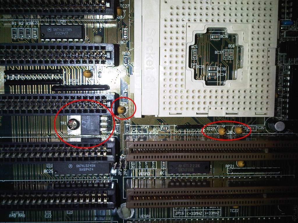
M104
- At least one rev M104 has been spotted with the 3-pin voltage regulator populated, but without the electrolytic capacitors at TC24, TC29 and TC30 (thanks to Chris Syntichakis for these pics). He also provided a pic of an unknown revision with the regulator plus caps.
M105
- Added support for Cyrix Cx486DX2V/DX4V (4-volt CPUs) and AMD Am486DX2/DX4 (3.3-volt CPUs) - JP24 and JP27 added for greater CPU voltage selection options.
- Voltage regulator socket is now 4-pin.
M106
- The silk-screened CPU type table has "P24D/M9" (M103 just calls this "P24D"), meaning this revision added support for the Cyrix 486 M9 (which later was renamed to "M1sc" and then again to 5x86).
- It also adds a seventh option, "P24T", which means this revision supports Intel Pentium OverDrive CPUs.
The Component Parts
The CPU Socket
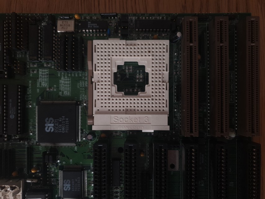 This being a Socket 3 motherboard and the presence of VESA Local Bus puts this board late in the 486-era. As such it supports both 3.3V and 5V CPUs (there are pads and a grounding plate for a voltage regulator just off one of the corners of the CPU socket). The available CPU options are:
From Intel: 80486SX, P23S (486SX SL Enhanced), DX, DX2, DX4, P24D (DX2 Write-back Enhanced), P24T (486DX4 OverDrive 5V), P24C (DX4 3.45V) and P24CT (Pentium OverDrive 3.3V).
From AMD: Am486DXL, DXL2 and SL.
From Cyrix (and other-branded equivalents from TI, IBM, and SGS): Cx486DX (M6), Cx486S2 and Cx486DX2 (M7).
From UMC: U5-S.
All of the above can be made to run from 25 MHz up to 100 MHz, making it a pretty useful motherboard to be installed in a retro PC if you are targeting anywhere in the 1989 to 1995 era. Note that the motherboard pre-dates both AMD 5x86 and Cyrix 5x86 (M1sc), so these are not supported. Another site says this board also supports P23T which is the Intel OverDrive 486SX2 and P4T which is the Intel OverDrive 486DX2.
According to the motherboard's silkscreen, it appears to be manufactured with the option of one of two system clock generators: either the IMI IMISC466 or the Macronix MX8315 (or its pin-compatible UMC UM9515) . Depending on which one your board has, you need to set the JP7 jumper differently. Mine has the IMI chip.
The Chipset
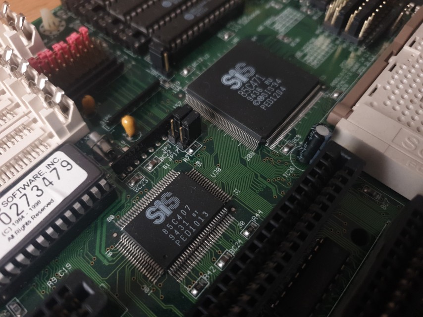 The motherboard uses the SiS 85C471/85C407 "Green PC" chipset, launched in early-to-mid-1994. This was their late-486 chipset. This two-chip chipset consisted of:
- 85C471 - CPU, Cache, Memory, ISA/VLB Bus Controller and Keyboard controller
- 85C407 - VLB to PCI Bridge
The chipset's key features include support for CPUs with a Write-Back L1 cache, up to 1 MB of L2 cache (though this board only supports up to 512 KB - see further down) and up to 128 MB of Fast Page Mode main memory (this board permits a maximum of 64 MB), programmable ISA bus speed, a hardware/software de-turbo switch, and power management modes.
Memory
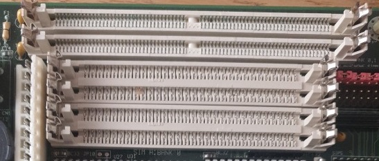 The motherboard has four 30-pin SIMM slots as well as two 72-pin SIMM slots, making up three "banks" in all - Bank 0 is the 30-pin ones (called "SIM A Bank 0"), with banks 1 and 2 above it (called "SIM B Bank 0 and 1"). Unlike most other boards, it will allow you to populate "SIM A" or "SIM B" independently. If populating only "SIM B", you must start populating Bank 0 before you populate Bank 1 (but you can only Bank 0, i.e. the first 72-pin slot, if you wish).
The maximum amount of memory supported by the Chaintech 4SLE is a whopping 64 MB. Even the fastest Pentiums (90 MHz) only shipped with 16 MB, so this mobo offers huge scope for expansion in the memory department.
The slots on the Chaintech 4SLE accept only the older "Fast Page Mode" (FPM) SIMMs, not the faster and newer "Extended Data Out" (EDO) SIMMs, sadly just missing the boat on this - EDO arrived in late 1993/early 1994 - so by the September 1994 date of this mobo, that is a shame. Still, EDO supposedly only gives about a 5% performance gain on FPM.
30-pin SIMM modules that work are 256 KB, 1 MB, 4 MB, and 16 MB (note: no 8 MB support), single- or double-sided. For the 72-pin SIMM slots, you can use 1 MB, 2 MB, 4 MB, 8 MB, 16 MB and 32 MB modules, but note that the memory config can be picky when mixing single-sided and double-sided SIMMs (single-sided came in 1 MB, 4 MB and 16 MB flavours, while double-sided came in 2 MB, 8 MB and 32 MB flavours).
Level 2 Cache
The motherboard supports 0, 64 KB, 128 KB, 256 KB, or 512 KB of Level 2 cache in its 2 banks, and they support bank interleaving. Bank 0 is the one closest to the corner of the board with Bank 1 closest to the memory slots. Here are the various cache configurations supported:
| Cache Size | Bank 0 | Bank 1 | Tag | Maximum Cacheable RAM |
|---|---|---|---|---|
| 64 KB | Four 8Kx8 | Four 8 Kx8 | One 8Kx8 | 16 MB |
| 128 KB | Four 32Kx8 | (Empty) | One 8Kx8 | 32 MB |
| 256 KB | Four 32Kx8 | Four 32Kx8 | One 16Kx8 or One 32Kx8 | 64 MB |
| 256 KB | Four 64Kx8 | (Empty) | One 16Kx8 or One 32Kx8 | 64 MB |
| 512 KB | Four 64Kx8 | Four 64Kx8 | One 32Kx8 | 128 MB* |
*This last option is pointless, since the board supports a maximum of 64 MB of RAM.
When I bought the motherboard it came fully populated with nine UMC UM61256AK-15 SRAM chips, which gives us 256 KB of L2 cache (the third configuration from the top, in the table above).
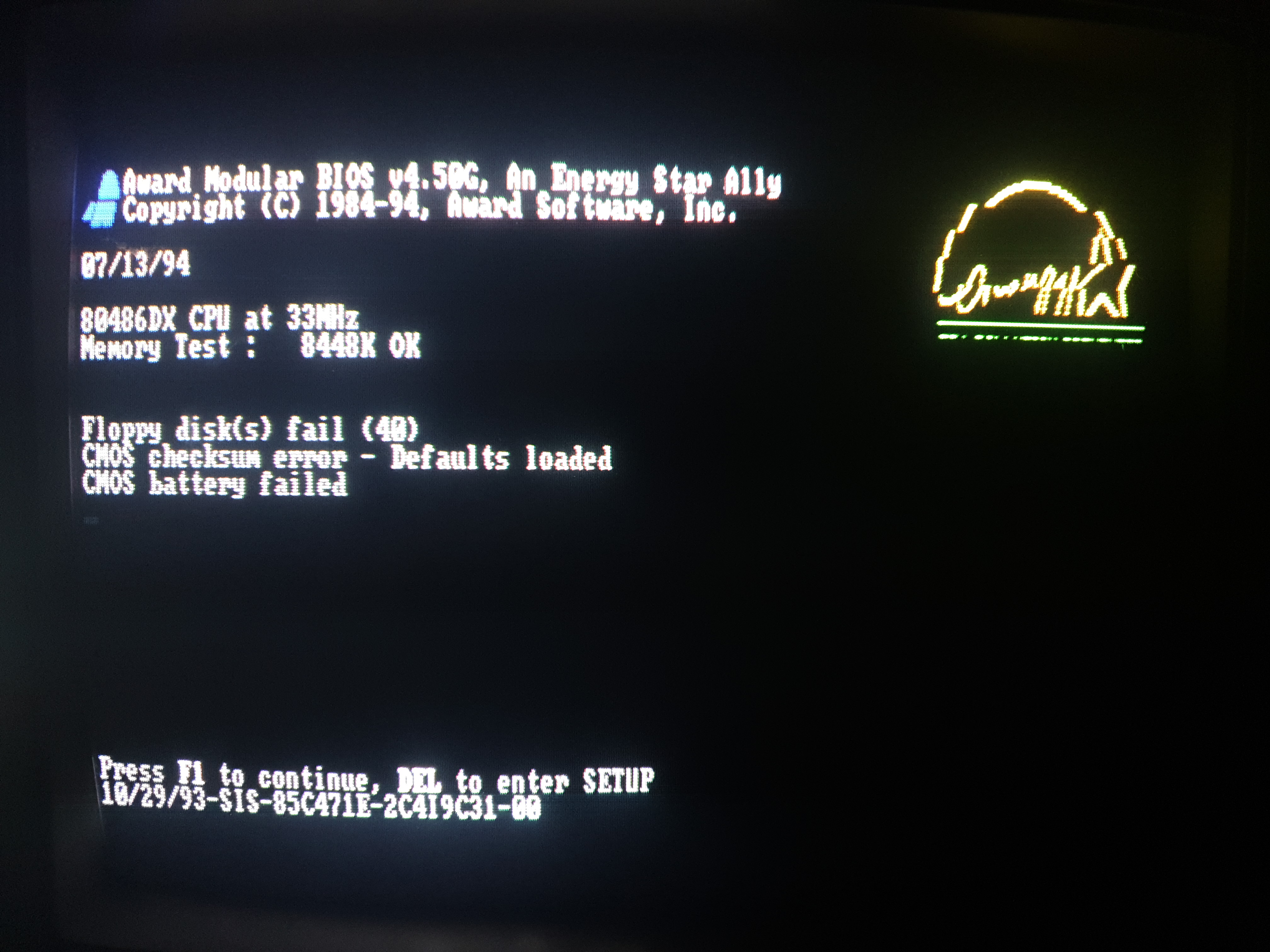
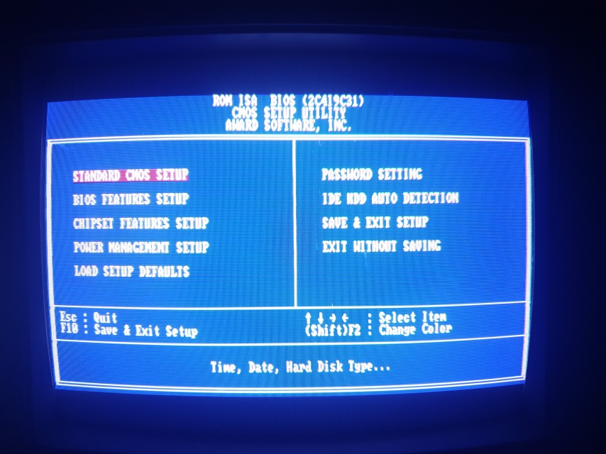
BIOS
My motherboard came with an Award Software core version 4.50G 486 BIOS, with a BIOS string of 10/29/93-SIS-85C471E-2C4I9C31-00. The "2C4I9" portion is the Award BIOS ID for the SiS 85C471B/E/G chipset of this board, and the added "C31-00" tells us it's a Chaintech 4SLE. Looking on the UltimateRetro.net website for other BIOS', it appears this board had these strings too:
11/13/94-SIS-85C471E-2C4I9C31-00 with a BIOS date of 11/24/9403/23/95-SIS-85C471E-2C4I9C31-00 with a BIOS date of 03/23/95
The BIOS chip is an ST Microelectronics M27C512, which is a 64 KB EPROM chip. You can download my 10/20/1993 BIOS dump here.
In a normal working system, the startup BIOS codes run as follows:
| Code* | Meaning | Notes |
|---|---|---|
| 05 04 | Keyboard controller self-tested. | Nothing shown on screen. |
| 0D 6F | Program some of the chipset's values, measure the CPU for display, and initialise the video. | VGA card's video BIOS string appears on the screen. |
| 0E 0D | Initialise the APIC (multiprocessor BIOS' only), determine startup screen message with CPU identification and speed. | (as above) |
| 0F 0E | DMA channel 0 tested | (as above) |
| 31 30 | Test base and extended memory, test base memory from 256KB-640KB, test extended memory above 1 MB. | "Award Modular BIOS v4.50G" message shown at top, and BIOS string at the bottom. Memory test begins. |
| 6F 40 6F 41 |
Initialise the floppy drive controller. | Floppy drive seek is heard. |
| 4E 48 4E 49 4E 4C 4E 4D |
Show all error messages found by the BIOS on screen, along with "Press F1 to continue, DEL to enter SETUP". | If any error messages are found, e.g. "Keyboard not found", "Floppy disk(s) fail (C0)", "CMOS checksum error -Defaults loaded", etc., the BIOS pauses waiting for you to press F1 or DEL. If no errors have been detected, the system waits about 5 seconds, then carries on. This BIOS code remains while you are in the BIOS. |
| 61 60 | Try to switch on the L2 cache | - |
| 61 5F | ? | - |
| FF 63 | Boot the system via Interrupt 19h. | System Configuration table is shown, and the system boots up. "BOOT DISK FAILURE, INSERT SYSTEM DISK AND PRESS ENTER" message appears. |
If it stops on any other codes (they're not always in numerical order if an error is detected), my advice is to try removing all expansion cards except a known-working VGA card and try again. Also confirm your memory sticks are working in another system.
It might be interesting to flash my BIOS with one of these to see what new additions were added - usually BIOS updates were released to either fix a bug or to allow a motherboard to support later CPUs.
I initially tested this board with an Intel 486DX2-66 and four OKI 256 KB 30-pin SIMMs in SIMM A
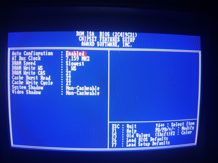
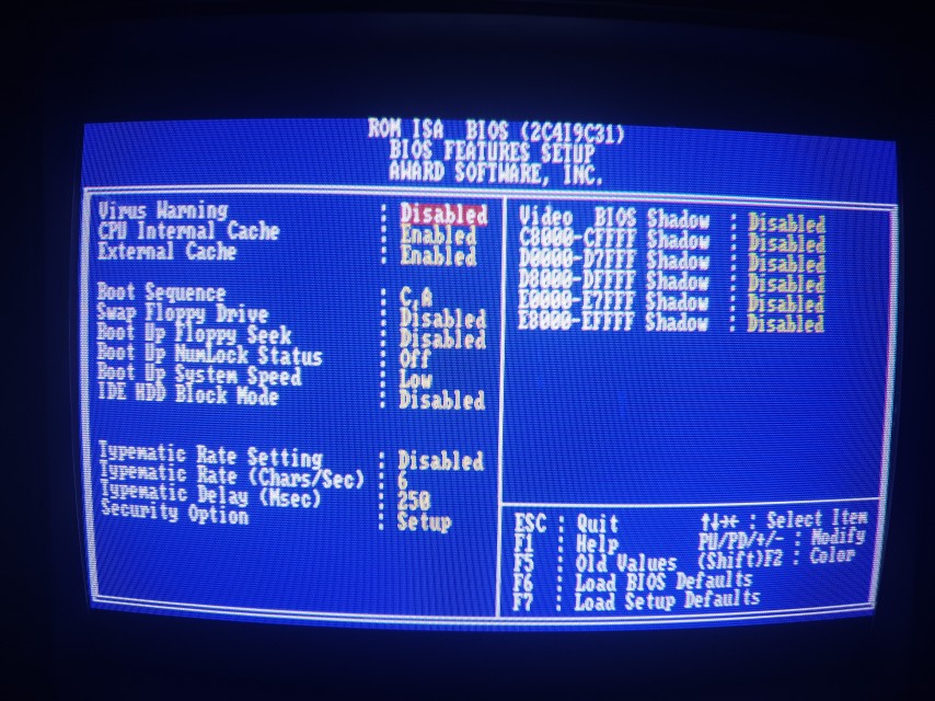
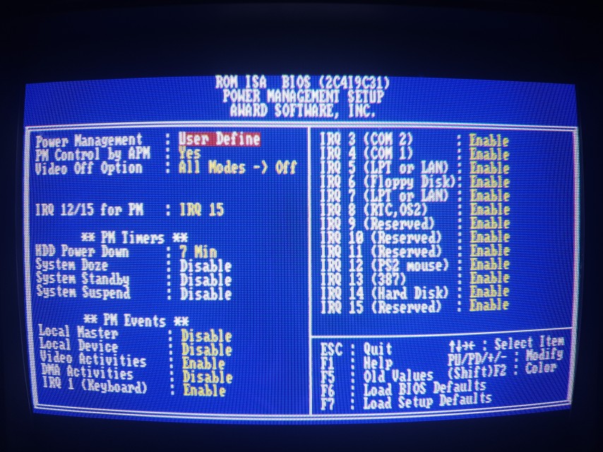
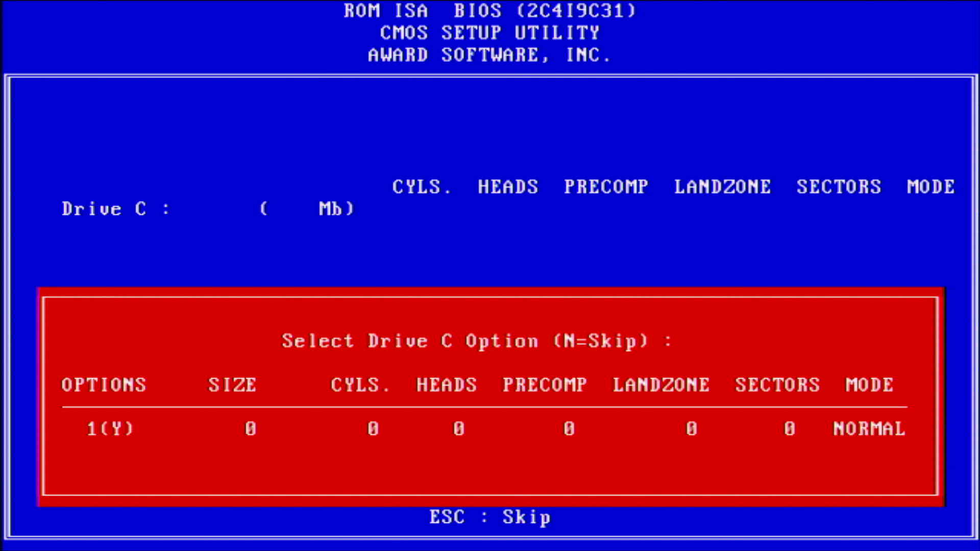
It's evident that the BIOS firmware has been upgraded, given the my BIOS date is now 07/13/94, so almost 9 months after it was manufactured. The BIOS does have a number of performance-improving options under its Chipset menu:
VESA Local Bus Slots
The three VESA Local Bus slots are what make this board special - late 486 boards like this existed at a time when graphics performance was in real demand. Premium PCs that got the new Intel Pentium processor would have PCI slots and a PCI graphics card while these mid-range boards came with VLB and a VLB graphics card. The VESA Local Bus is able to drive a VLB graphics card at 33 MHz instead of the ISA bus's sedentary 8 MHz.
In Part 2, we'll mess with those bazillion jumpers and put it through its paces