Cache Explained
A cache in computer terms is a small amount of fast memory that stores frequently used information, so that if that same information is required again (shortly after) it can be retrieved more quickly, thus improving performance of the system.
This page gives a very brief overview of caches in PCs throughout the 80s and 90s, without going into much technical detail. There are numerous resources online that better explain how and why caches are designed the way they are.
There are often several caches found in a DOS or early Windows PC:-
Level1 (L1) cache - inside the CPU die.
Level2 (L2) cache - on the motherboard.
For DOS PCs, caching became more important as time grew on. The early PCs (up to and including 80386) had no cache at all. All memory operations would go from the CPU out to main memory and then back again.
L1 Cache
Starting with the launch of the Intel 486DX in 1989, Intel embedded a very small cache within the CPU itself. It was 8 KB in size, and in later generations would be referred to as the "level 1" cache to disinguish it from other caches in the computer. The CPU itself would keep track of frequently used operations and store them in this cache. Because of the close proximity of the cache to the CPU that was calling it, the CPU would have very quick access to the information stored in there (it takes fewer clock cycles to communicate with the L1 cache than using any external memory bus on the motherboard), so if the same instruction was detected again, it would retrieve the information from the cache instead of going all the way out to main memory which was a much slower operation.
L2 Cache
 As motherboard manfacturers adopted the 486 CPU, they began to include a secondary cache on the motherboard, which they called the "level 2" (L2) cache. This would still be accessible more quickly than main memory primarily because the cache chips are specified to be faster, for example these SRAM chips would have access times of around 15 or 20ns (nanoseconds) rather than 70ns that main memory would typically run at. They would also be larger in capacity than the L1 cache.
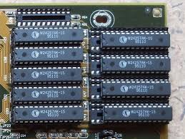
28-pin SRAM chips could provide an individual capacity of up to 32 KB. Later, 32-pin SRAM chips came on the scene, able to hold a capacity of up to 512 KB each. 28-pin SRAMs are pin-compatible with 32-pin cache sockets, as you can see in the picture above - just be sure to align and orient them correctly!
Like main memory at the time, cache memory sometimes came in 'banks', where each bank would need to be populated in full (or not at all) for the board to work. Cache banks like in the picture above would also sometimes include one or two "Tag" RAM sockets, one socket per bank of cache chips. The purpose of the tag RAM in conjunction with what is called a "comparator" is to detect the cache hit/miss status by comparing the high-order address bits for the current memory cycle with the stored "tag" bits from previous cache entries. When a match is detected and the location is cacheable, a cache hit cycle occurs. If no match, the current cycle is a cache miss. Essentially, having Tag RAM chips as well improves performance further.
In some cases, a motherboard would have a dedicated cache expansion slot (called a "COAST" slot) that takes an add-on card which contains the cache chips on it. Some motherboards have both cache RAM chips on the board and a cache expansion slot to further expand the size of the L2 cache.
Ideal Cache Size to Main Memory Size
Certain cache sizes are "ideal" for a given amount of memory. You might notice that on some 386 and 486 motherboards that can support a maximum of 32 MB of RAM, there is 128 KB of cache included but space to add another 128 KB. So if you brought up the cache size to the full 256 KB for 32 MB of memory it would yield an improvement in the cache "hit ratio" and thus overall memory performance. There are diminshing returns, however - With 32 MB of main memory, adding another 256 KB of cache (making 512 KB total cache size) would increase the hit ratio only by roughly another 10%.
Now if you have less than the ideal amount of cache for a given RAM size, say 256 KB of cache for 128MB of RAM, your hit ratio will decrease, as you have a small amount of cache trying to cache a large amount of memory. As I said, for 128MB, 512 KB of cache is ideal - if you have only half this much (256 KB) the cache will 'miss' much more often and you will lose performance. So here are the ideals of cache size to main memory size:
| Main Memory | L2 Cache Size in Write-Back Mode | L2 Cache Size in Write-Through Mode | Tag RAM Size |
|---|---|---|---|
| 8 MB | 64 KB | 32 KB | 8Kx8 chip |
| 16 MB | 128 KB | 64 KB | 8Kx8 chip |
| 32 MB | 256 KB | 128 KB | 8Kx8 chip |
| 64 MB | 512 KB | 256 KB | 16Kx8 chip |
| 128 MB | 1024 KB | 512 KB | 32Kx8 chip |
Ideal L2 cache size compared to main memory size
The main reason to go from 128 KB to 256 KB of cache is more to do with cache bank interleaving than improving the cache hit ratio. Many chipsets support bank interleaving which can significantly improve performance.
The cacheable area (of main memory) also depends on the size of your Tag RAM chip(s) and the mapping scheme employed by your motherboard's chipset, which is explained further down.
Note that Write-Back (WB) cache mode effectively halves the amount of cacheable area, since this mode caches writes as well as reads, so twice as much cache is needed to support the same amount of main memory. For systems that support WB mode, definitely use it, and be sure to have a minimum ratio of 128:1 (main memory KB to cache memory KB). If your motherboard chipset only supports Write-Through (WT) mode, use a ratio of 256:1 (main memory KB to cache memory KB).
The formula you can use to calculate the total amount of cacheable memory is something like this:
In a configuration of 64 KB of L2 cache, this has 4096 (2^16 bytes / 2^4 bytes per line) cache lines each of 16 bytes (because a 386 or 486 uses four 32-bit words) - resulting in a [line:byte] address of [12:4] = 16 bits long.
Add to that, in WT mode, 8 bits that the tag stores and you get a [tag:line:byte] of [8:12:4] address which is 24 bits in length and thus 16 MB are addressable by the cache in total.
Here are the sums for other L2 common cache sizes:
L2 Cache = 128 KB
Cache Line Size = 16 bytes
# Cache Lines
= (2^17 / 16 bytes per line) = 131072 / 16 = 8192
Cache Address Length = 8 bits of tag, 13 bits for the line and 4 bits for byte = 25 bits long
Maximum Cacheable Memory (WT mode) =
32 MB
L2 Cache = 256 KB
Cache Line Size = 16 bytes
# Cache Lines
= (2^18 / 16 bytes per line) = 262144 / 16 = 16384
Cache Address Length = 8 bits of tag, 14 bits for the line and 4 bits for byte = 26 bits long
Maximum Cacheable Memory (WT mode) =
64 MB
L2 Cache = 512 KB
Cache Line Size = 16 bytes
# Cache Lines
= (2^18 / 16 bytes per line) = 524288 / 16 =32768
Cache Address Length = 8 bits of tag, 15 bits for the line and 4 bits for byte = 27 bits long
Maximum Cacheable Memory (WT mode) =
128 MB
Use this chart to see the make-up of cache address capacity at different sizes:

To measure the tag RAM size needed:
Cache = 128 KB: 2^17 / 2^4 (16 bytes) = 2^13 (8192) = 8 KB tag chip
Cache = 256 KB: 2^18 / 2^4 (16 bytes) = 2^14 (16384) = 16 KB tag chip
Cache = 512 KB: 2^19 / 2^4 (16 bytes) = 2^15 (32768) = 32 KB tag chip
Cache = 1024 KB: 2^20 / 2^4 (16 bytes) = 2^16 (65536) = 64 KB tag chip
Bear in mind there is no compelling reason to have more than 64 MB of main memory for DOS or Windows 95, so why take a performance hit?
Cache Mapping Types
There are 3 types of mapping used in early PCs with caches
- Direct mapped
- Associative mapped
- Set-associative mapped
Direct mapping is the simplest - it maps each block of main memory to only 1 possible line in the cache. If a line is already taken up by a memory block when a new block needs to be loaded, the old block is removed from the cache. An address space is split into 2 parts: an index field and a tag field. The cache is used to store the tag field, whereas the index field is stored in main memory. Direct mapped performance is directly proportional to the cache hit ratio.
With Associative mapping, any block can go into any line of the cache. It is considered to be the fastest and most flexible mapping type.
Set-Associative mapping is an enhanced form of direct mapping where the drawbacks of direct mapping are removed. Instead of having exactly one line that a block can map to in the cache, it groups a few lines together to create a set. Then a block in memory can map to any one of the lines of a specific set. Set-associative mapping allows that each word that is present in the cache can have two or more words in the main memory for the same index address. Set associative cache mapping combines the best of direct and associative cache mapping techniques.
The Size vs Cost Trade-Off
L1 caches are typically small because the silicon on which the CPU and its L1 cache are made is very expensive. The larger the cache, the more area on the silicon it takes up (more transistors are needed to store the information), which directly translates into a higher cost to build the CPU.
L2 caches can be larger simply because they are stored in cheaper ICs (chips) that are soldered or socketed on the motherboard, where physical space is not so much of an issue. During the 486 era, motherboards would typically come with anywhere from 0 to 512 KB of level 2 cache. Often they would be sold with half the L2 cache sockets populated, leaving the buyer to have the choice of purchasing more later.
Technical Explanation
Note: The following text is a subset of a response given on the Superuser.com forum by user Hennes, and all credit goes to him for this detailed but readable answer. I have only made minor alterations to correct grammar and spelling:-
To understand caches you need to know a few things:
A CPU has registers - values held in these can be directly used. Nothing is faster. However we cannot add infinite registers to a chip. These things take up space. If we make the chip bigger it gets more expensive. Part of that is because we need a larger chip (more silicon), but also because the number of chips with problems will then increase.
(Take an imaginary [silicon] wafer of size 500 cm2. I cut 10 chips from it, each chip is 50cm2 in size.
One of them is broken, so I discard it and I am left with 9 working chips.
Now take the same wafer and cut 100 chips from it, each ten times as small.
One of them is broken. I discard the broken chip and I am left with 99 working chips.
That is a fraction of the loss I would otherwise have had. To compensate for the larger chips I would need to ask higher prices. More than just the price for the extra silicon).
This is one of the reasons why we want small, affordable chips. However the closer the cache is to the CPU, the faster it can be accessed.
This is also easy to explain: electrical signals travel a near light speed. That is fast but is still a finite speed. Modern CPUs work with GHz clocks. That is also fast. If I take a 4 GHz CPU then an electrical signal can travel about 7.5cm per clock tick. That is 7.5 cm in straight line (chips are anything but straight connections). In practice you will need significantly less than those 7.5 cm since that does not allow any time for the chips to present the requested data and for the signal to travel back.
Bottom line: we want the cache as physically as close as possible. Which means large chips.
These two need to be balanced (performance vs. cost).
Where exactly are the L1, L2 and L3 Caches located in a computer?
Assuming PC-style only hardware (mainframes are quite different, including in the performance vs. cost balance):-
IBM XT (1981)
The original 4.77Mhz one: No cache. CPU accesses the memory directly. A read from memory would follow this pattern:
- The CPU puts the address it wants to read on the memory bus and asserts the read flag.
- Memory puts the data on the data bus.
- The CPU copies the data from the data bus to its internal registers.
80286 (1982)
Still no cache. Memory access was not a big problem for the lower speed versions (6Mhz), but the faster model ran up to 20Mhz and often needed to delay (using "wait states") when accessing memory.
You then get a scenario like this:
- The CPU puts the address it wants to read on the memory bus and asserts the read flag.
- Memory starts to put the data on the data bus.
- The CPU waits.
- Memory finishes getting the data and it is now stable on the data bus.
- The CPU copies the data from the data bus to its internal registers.
That is an extra step spent waiting for the memory. On a modern system that can easily be 12 steps, which is why we have cache.
80386 (1985)
The CPUs get faster. Both per clock (more efficient), and by running at higher clock speeds.
RAM gets faster, but not at the same rate as the CPU.
As a result more wait states are needed. Some motherboards work around this by adding cache (that would be 1st level cache) on the motherboard.
A read from memory now starts with a check if the data is already in the cache. If it is, the data is read from the much faster cache. If not, the same procedure is as described with the 80286.
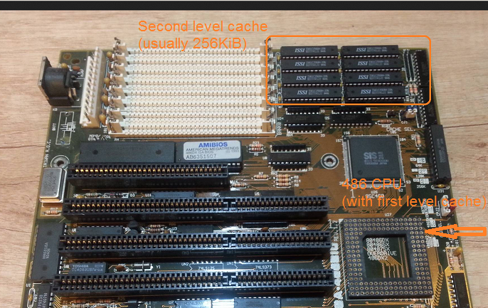
80486 (1989)
This is the first CPU for PCs which has some cache on the CPU.
It is an 8 KB "unified" cache which means it is used for both data and instructions.
Around this time it gets common to put 256 KB of fast static memory on the motherboard as 2nd level cache. Thus 1st level cache is on the CPU, 2nd level cache is on the motherboard.
Pentium (1993)
The 586, or Pentium 1, uses a split-level 1 cache, 8 KB each for data and instructions. The cache was split so that the data and instruction caches could be individually tuned for their specific use. You still have a small yet very fast 1st cache near the CPU, and a larger but slower 2nd cache on the motherboard (at a larger physical distance).
In the same Pentium 1 era Intel produced the Pentium Pro. Depending on the model, this chip had a 256 KB, 512 KB or 1 MB on-board cache. It was also much more expensive, which is easy to explain with the following picture.
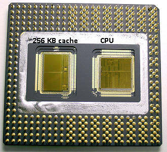
Notice that half the space in the chip is used by the cache. And this is for the 256 KB model. More cache was technically possible and some models were produced with 512 KB and 1 MB caches. The market price for these was high.
Also notice that this chip contains two dies. One with the actual CPU and 1st cache, and a second die with 256 KB 2nd cache.
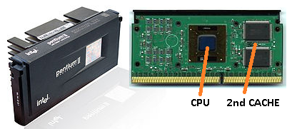
Pentium II (1997)
The Pentium II has a Pentium Pro core. For economy reasons no 2nd cache is in the CPU. Instead what is sold as a "CPU" is a PCB [printed circuit board] with separate chips for CPU (and 1st cache) and 2nd cache.
As technology progresses and we start to create chips with smaller components it gets financially possible to put the 2nd cache back in the actual CPU die. However there is still a split. Very fast 1st cache snuggled up to the CPU. With one 1st cache per CPU core and a larger but less fast 2nd cache next to the core.
Pentium 3 & 4
This does not change for the Pentium 3 or the Pentium 4.
Around this time we have reached a practical limit on how fast we can clock CPUs. An 8086 or a 80286 did not need cooling. A Pentium 4 running at 3.0GHz produces so much heat and uses that much power that it becomes more practical to put two separate CPUs on the motherboard rather than one fast one (two 2.0 GHz CPU's would use less power than an single identical 3.0 GHz CPU, yet could do more work).
This could be solved in three ways:
- Make the CPUs more efficient, so they do more work at the same speed.
- Use multiple CPUs.
- Use multiple CPUs in the same 'chip'.
1) Is an ongoing process. It is not new and it will not stop.
2) Was done early on (e.g. with dual Pentium 1 motherboards and the NX chipset). Until now that was the only option for building a faster PC.
3) Requires CPUs where multiple 'cpu core' are built into a single chip. We then called that CPU a dual core CPU to increase the confusion. Thank you marketing :) These days we just refer to the CPU as a 'core' to avoid confusion.
You now get chips like the Pentium D (duo), which is basically two Pentium 4 cores on the same chip.
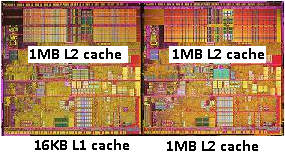
Remember the picture of the old Pentium Pro? With the huge cache size? See the two large areas in this picture?
It turns out that we can share that 2nd cache between both CPU cores. Speed would drop slightly, but a 512 KB shared 2nd cache is often faster than adding two independent 2nd level caches of half the size. It means that if you read something from one CPU core and later try to read it from another core which shares the same cache that you will get a cache hit. Memory will not need to be accessed.
Since programs do migrate between CPUs, depending on the load, the number of the core and scheduler you can gain additional performance by pinning programs which use the same data to the same CPU (cache hits on L1 and lower) or on the same CPUs which share L2 cache (and thus get misses on L1, but hits on L2 cache reads). Thus on later models you will see shared level 2 caches.