Retro Review: Orchid Fahrenheit VA/VLB Card
7th January 2023
Back in 2014 I acquired this Orchid Fahrenheit VA/VLB SVGA card as part of a bundle of four graphics cards for the princely sum of £48.
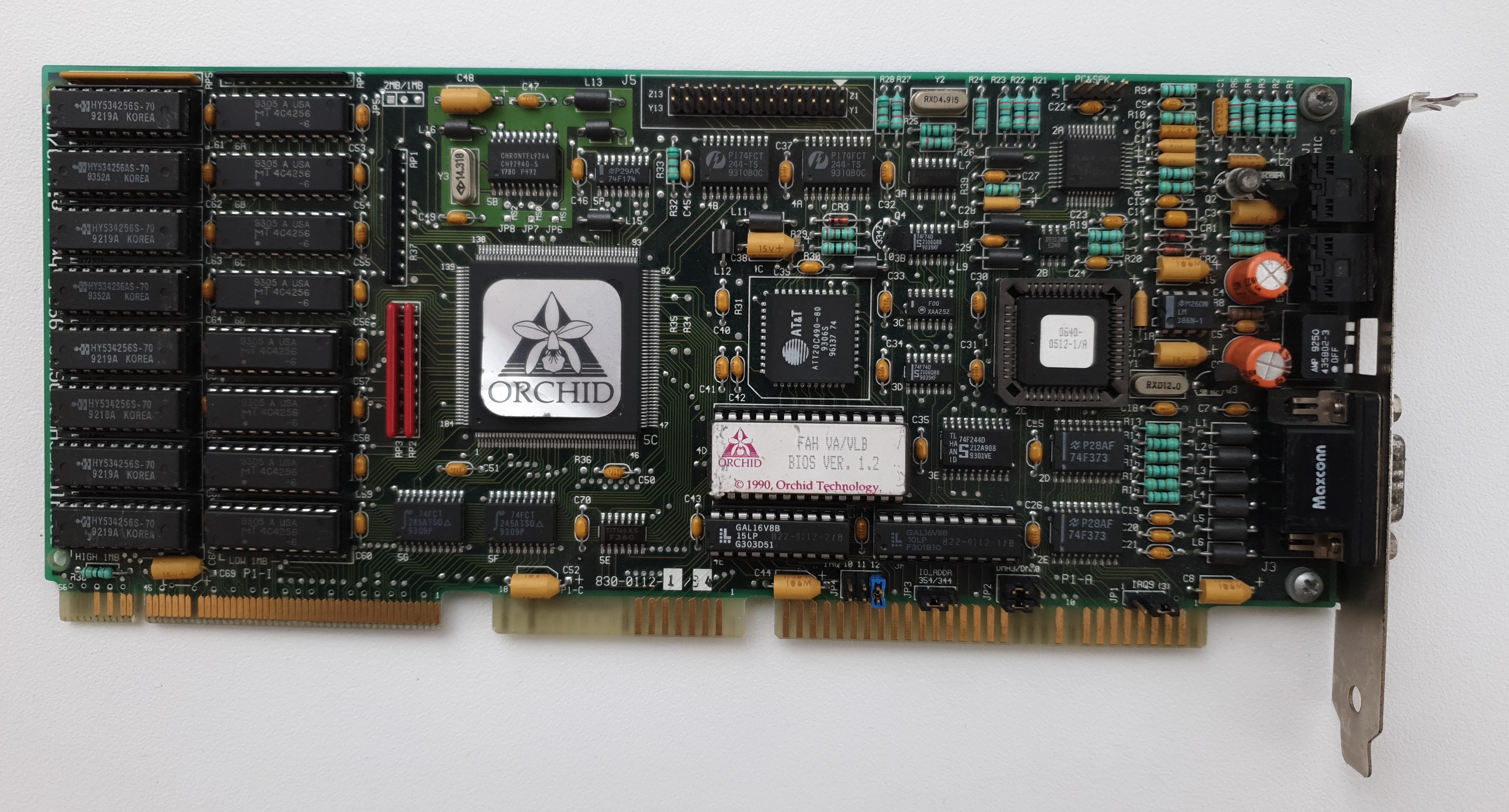
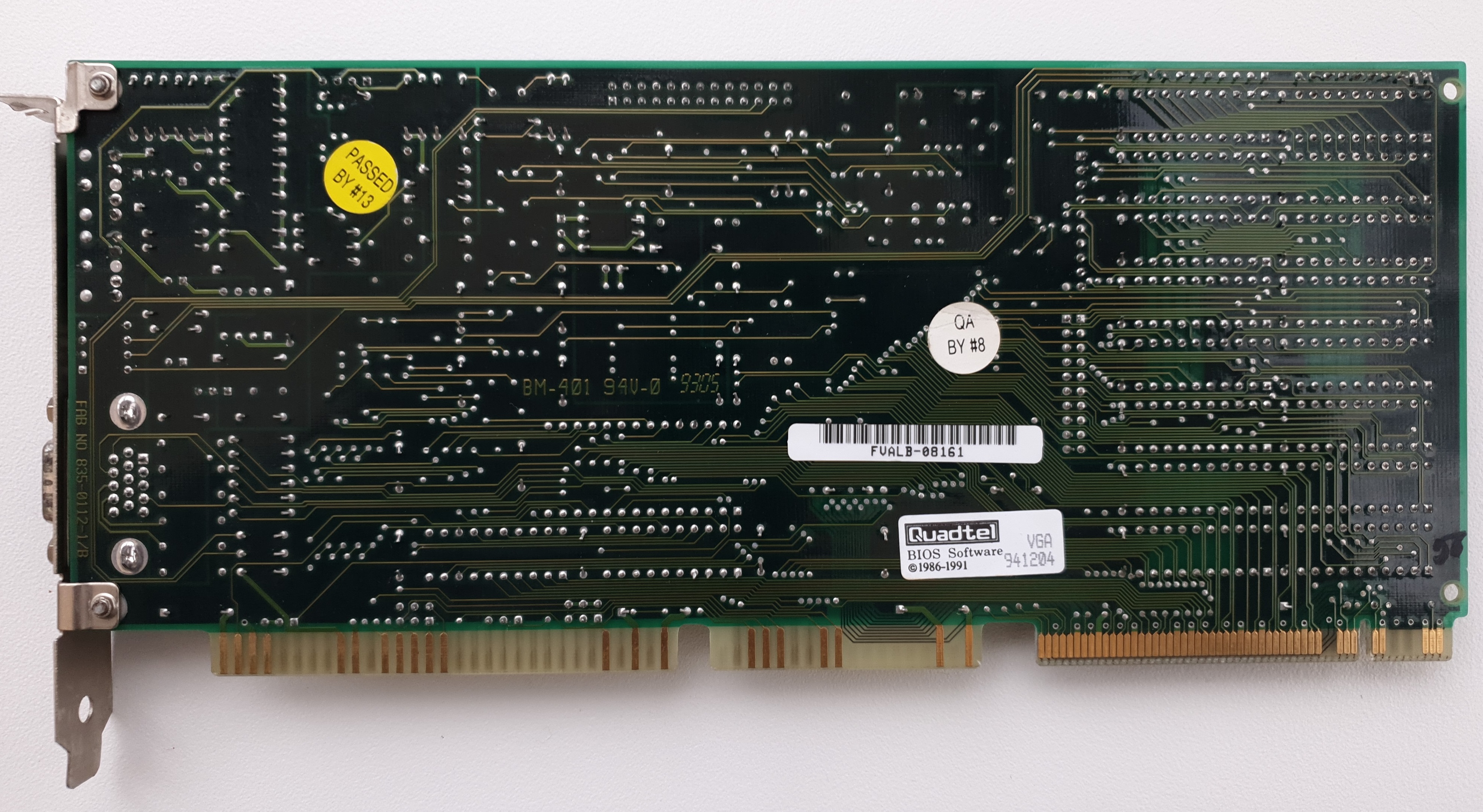
Orchid Fahrenheit VA/VLB Super VGA card, ca. 1992
This was the first VESA Local Bus graphics card I added to my collection - the only other VLB card in my collection was a cheap Pine Technology multi-I/O card that I got with a Time Computers PC I bought around 2000 in the UK. I was keen to finally look into the performance benefits of the 32-bit VESA Local Bus over 16-bit ISA architecture from a gaming perspective.
The Fahrenheit VA/VLB was an interesting and somewhat unique combination of a graphics card coupled with audio capabilities, though the latter is not for gaming. The "VA" in the name stands for "Voice Activated" - aimed at business users looking to control their PC via a microphone. The card came with Orchid's Voice Notes software that allowed you to speak words which it could then store as voice annotations to any Windows application. As we now know, this concept never really caught on, but it is interesting to look back on it as an idea.
The VA/VLB came out at the same time as the Fahrenheit VA, which was the 16-bit ISA version. The Fahrenheit 1280 Plus which came out a year later has exactly the same board design but is missing all the audio components.
This review will focus on the card's graphics capabilities and gaming performance, and if I get the time I'll also give its audio aspects a try.
What's on the Board?
So what component parts make up this nice little graphics card that's bustling with chips? It appears to have:
- A large ASIC with an Orchid sticker on top.
- An ATT20C490 RAMDAC.
- 2 MB of video memory in sixteen 256k x 4 DRAM chips.
- A 28-pin EPROM containing the BIOS.
- A soldered-in 44-pin chip which I assume is the main audio chip.
- A 44-pin socketed chip.
- A Chrontel CH9294 clock generator.
- A 26-pin VESA feature connector at the top of the card.
- A 4-pin header marked PC&SPK
- 4 DIP switches on the side.
- A 9-pin D-SUB on the faceplate for digital video out .
- Two 3.5mm jack sockets on the faceplate: MIC (top one) and SPEAKER (bottom one).
- 4 jumpers in the lower-right corner.
Video Controller
The main ASIC is an S3 P86C805 - the Super VGA chipset. This is the VESA Local Bus variant of the ISA-based 86C801.
.jpg) The S3 86C801 and 86C805 came out in 1993. It was their second generation of Windows accelerators after their first-gen chips, the 911 and 924. Both the 801 and 805 are known for their excellent performance in DOS and Windows, and cards based on this chipset were reasonably-priced when they arrived.
The S3 86C801 and 86C805 came out in 1993. It was their second generation of Windows accelerators after their first-gen chips, the 911 and 924. Both the 801 and 805 are known for their excellent performance in DOS and Windows, and cards based on this chipset were reasonably-priced when they arrived.
The 86C805 is 32-bit internally and connects to its video memory using a 32-bit wide data path, all operating in zero wait states. This was the main reason for its high performance. Note that the ISA-based 86C801 is the same core but communicates with video memory via a 16-bit wide data path.
The 86C805 can output these resolutions and colour depths:
- 1,280 x 1,024 in 256 colours (on 2 MB cards like mine here) or 16 colours (on a standard 1 MB card)
- 1,024 x 768 in 256 colours (1 MB card, 72 Hz refresh rate non-interlaced)
- 800 x 600 in 32,768 colours (2 MB card)
- 640 x 480 in 16.7 million colours (1 MB card)
RAMDAC
The RAMDAC chip is an AT&T ATT20C490 running at 80 MHz.
.jpg) This is a 24-bit (TrueColor) DAC offering 16.7 million colours, and is pin- and function-compatible with the ATT20C491/492, which were more enhanced versions that added gamma correction and a few other niceties.
This is a 24-bit (TrueColor) DAC offering 16.7 million colours, and is pin- and function-compatible with the ATT20C491/492, which were more enhanced versions that added gamma correction and a few other niceties.
It was available in 66, 80, 100 and 110 MHz speeds.
Some other Fahrenheit VA/VLB cards I have seen have a Sierra Semiconductor SC15025CV HICOLOR-24 RAMDAC in this location, also running at 80 MHz.
Video Memory
.jpg) These cards were sold with 1 MB of video memory, but were expandable to a maximum of 2 MB. Bank 0 is the one closest to the main chip and bank 1 (usually empty sockets) is the one nearest the edge of the card. The only DRAM chips the card will accept are 256Kx4.
These cards were sold with 1 MB of video memory, but were expandable to a maximum of 2 MB. Bank 0 is the one closest to the main chip and bank 1 (usually empty sockets) is the one nearest the edge of the card. The only DRAM chips the card will accept are 256Kx4.
My card has been expanded to 2 MB, but interestingly this second bank is installed with slower 70ns DRAM chips compared to the factory ones in bank 0 that are 60ns. I believe the card will only run at the speed of the slowest memory, so this expansion would have slightly throttled the card's performance even though it would have opened up the ability to display at higher resolutions.
There is a jumper, JP5, that is supposedly used to tell the card whether 1 MB or 2 MB is installed, but there is no pin header. Looking at unexpanded versions of this card there is still no pin header so this jumper is probably not needed on the VA or VA/VLB, but since this board design is shared with the Fahrenheit 1280, perhaps it's used there.
Some Fahrenheit 1280 Plus and Fahrenheit VA/VLB cards appear to have 50ns DRAMs which are extremely rare!
I do have another set of eight 60ns DRAMs that I purchased for my Fast 286 review, so when I benchmark this card I'll be sure to swap out these 70's for the 60's to see if it makes a difference in gaming performance.
VGA BIOS
.jpg) The VGA BIOS chip is marked 'FAH VA/VLB BIOS VER 1.2'. It's a 28-pin EPROM chip, most likely of 32 KB capacity.
The VGA BIOS chip is marked 'FAH VA/VLB BIOS VER 1.2'. It's a 28-pin EPROM chip, most likely of 32 KB capacity.
There are several versions of the BIOS for this card, including:
- V1.1 (on a Fahrenheit VA ISA card)
- V1.2 (my card)
- V1.3 (on Fahrenheit 1280 Plus ISA and 1280 Plus/VLB cards)
- V2.0 (on Fahrenheit 1280 Plus ISA and 1280 Plus/VLB cards)
- V3.0 (on a Fahrenheit VA/VLB card)
The copyright year is meaningless on these chips, as the VA and VA/VLB cards didn't come out until in 1992 and 1993 respectively (the Fahrenheit 1280 was 1991 and 1280 Plus was 1993), and most of these versions have a "(C) 1990" text on them! Orchid must have just used stickers they had lying around. I don't know if the BIOS is interchangeable between the VA or VA/VLB and the 1280 Plus. I would guess swapping between a VA and VA/VLB card would work, but the 1280 Plus might not.
Main Audio Chip
.jpg) The small, soldered-in 44-pin chip in the top-right corner of the card is an OKI M6388. I did some digging to locate the datasheet, and it turns out the full part number is MSM6388 - it's a Solid State Recorder IC.
The small, soldered-in 44-pin chip in the top-right corner of the card is an OKI M6388. I did some digging to locate the datasheet, and it turns out the full part number is MSM6388 - it's a Solid State Recorder IC.
Interestingly, the same location on the Fahrenheit 1280 [which shares the same board layout] has solder pads with "ES488" etched in the middle, and on the Fahrenheit 1280 Plus it's etched "MSM638". On another Fahrenheit VA/VLB, the chip there is actually an "ES488", so presumably this OKI chip is interchangeable with the ESS ES488 AudioDrive chip! It's a shame they didn't extend this card's functionality to fully leverage the ES488's Ad Lib and Sound Blaster-compatibility.
Microcontroller Chip
.jpg) Again, the 1280 comes to our rescue to help identify what this chip is. On that card which just has solder pads in this location report it as being for a 65512, full name MSM65512. It turns out this is an 8-bit microcontroller.
Again, the 1280 comes to our rescue to help identify what this chip is. On that card which just has solder pads in this location report it as being for a 65512, full name MSM65512. It turns out this is an 8-bit microcontroller.
Some Fahrenheit VA/VLB board revisions have this chip while others do not. My card has a board revision 830-0112-1/B, and of course has this additional chip. A later revision is 830-0112-5/C4 and has the ESS ES488 but no microcontroller. It is also missing one of two GAL16V8B programmable gate array chips and some of the other glue logic that my card has. For the ISA version of the card, board revision 830-116-1/C1 has the same OKI M6388 and also this microcontroller, so perhaps if you have the OKI it needs to be supplemented with this microcontroller too, but if you have a version with the ES488 it doesn't?
Configuring the Card
The 4 DIP switches on the side of the card have the following configurations:
SW1 and SW2 set the refresh rate for the specific resolution you are running in, as follows:
| SW1 | SW2 | @ 640 x 480 | @ 800 x 600 | @1,024 x 768 | @1,280 x 960 | @1,280 x 1,024 |
|---|---|---|---|---|---|---|
| OFF | OFF | 72 Hz | 72 Hz | 60 Hz NI | 43 Hz I | 43 Hz I |
| ON | OFF | 72 Hz | 72 Hz | 70 Hz NI | 43 Hz I | 43 Hz I |
| OFF | ON | 60 Hz | 56 Hz | 43 Hz I | - | - |
| ON | ON | 60 Hz | 60 Hz | 60 Hz NI | - | - |
SW3 is factory configured and should not be changed.
SW4 sets the speaker type this is attached:
| SW4 | Speaker Type |
|---|---|
| OFF | Mono |
| ON | Stereo |
In addition to the DIP switches, the audio portion of the card has three jumpers:
| Jumper | Meaning | Settings |
|---|---|---|
| JP2 | DMA Channel | Pins 1-2 & 4-5 closed: DMA Channel 3 Pins 2-3 & 5-6 closed: DMA Channel 0 Note: pin 1 is the top-left, pin 4 is below it. |
| JP3 | I/O Address | Pins 1-2 closed: 354h Pins 2-3 closed: 344h Note: pin1 is the leftmost pin |
| JP4 | IRQ | Left two pins closed: IRQ 10 Middle two pins closed: IRQ 11 Right two pins closed: IRQ12 |
In Part 2 (hopefully out sometime also in January 2023, as I've hit a snag where all my VLB motherboards are currently inoperable - ugh...) I will install the card, install any drivers and utility software, and begin benchmarking!