The Faraday FE2010A Chipset
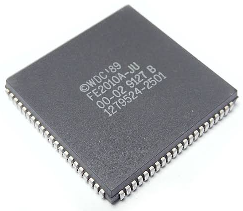 Originally designed and sold in the late 1980s and early 1990s, the Faraday FE2010A was a single-chip chipset for XT machines. I have a clone of this chip on my first XT computer that I bought back in 1991 - my chip is the Proton PT8010AF. The chip itself is a 2 micron CMOS gate array with 84 pins and is in a J-leaded PLCC (Plastic Leaded Chip Carrier) package.
Faraday Electronics were originally founded in 1982 and had their headquarters in Sunnyvale, CA. They also made several other single-chip chipsets including the FE2011 which was designed for clones of the IBM PS/2 Model 30 (8086/80C86/V30-based), an AT single-chip chipset called FE3000A, a four-IC chipset called FE3600 (for 286 and 386SX systems), and a clone of the PS/2 Models 50 and 60 called FE5400.
Much of the information on this page has come from another source on the web here: https://github.com/skiselev/micro_8088/blob/master/Documentation/Faraday-XT_Controller-FE2010A.md
Manufactured by Western Digital after they bought Faraday Electronics in July 1987, the FE2010A was an enhanced version of their earlier FE2010 controller, with the key difference being support for Turbo mode, i.e. higher clock speeds. The chipset implements all of the Intel 8xxx supporting ICs (excluding the CPU and FPU) as well as all the glue logic chips found on the IBM XT motherboard, including:
- Intel 8288 Bus controller
- Intel 8042 Clock generator
- Intel 8259A Interrupt controller
- Intel 8237A DMA controller
- Intel 8253 Timer
It claimed to be able to reduce the size of an XT motherboard by 77%, and reduce the component count by 71 pieces!
The datasheet for the FE2010 is here. I was unable to find a datasheet for the FE2010A, but the differences are minimal.
PCs known to have used the FE2010, FE2010A or a clone of them are:
- Commodore PC-1 5 MHz - FE2010 in position U10.
- Commodore PC-1 10 MHz - FE2010A in position U10.
- Commodore PC-10-III - FE2010A in position U101.
- Commodore PC-20-III - FE2010A in position ?.
- Morgan Generic Base XT - Proton PT8010AF in position U1.
- Micro 8088 project (by Skiselev)
- GEM Computer Products GEM-10 - FE2010A in position U4.
The original FE2010 only supported Intel 8088 up to 4.77 MHz using a 14.31818 MHz crystal oscillator. The FE2010A supports both 4.77 MHz and 7.15 MHz clock frequencies using the same crystal. It can also support 4.77, 7.15 and 9.54 MHz CPU clock frequencies with the use of a 28.63636 MHz crystal. Pin 16 (XSEL) on the FE2010A is used to indicate the crystal frequency:
- 14.31818 MHz crystal oscillator - pin 16 pulled up, e.g. connected to +5V using a 4.7 kohm resistor
- 28.63636 MHz crystal oscillator - pin 16 pulled down, e.g. connected to the ground
There also seems to be a difference in the way the Faraday FE2010A implements the DRAM controller: The FE2010 had only a single bit in the Configuration Register to set the DRAM size, while the FE2010A implements two such bits.
I/O Address Map
| Address | I/O Resource |
|---|---|
| 0x00 - 0x0F | 8237-compatible DMA Controller |
| 0x10 - 0x1F | Reserved |
| 0x20 - 0x21 | 8259-compatible Interrupt Controller |
| 0x22 - 0x3F | Reserved |
| 0x40 - 0x42 | 8253-compatible Timer |
| 0x44 - 0x5F | Reserved |
| 0x60 | Keyboard Data Register |
| 0x61 | Control Register (aka Port B) |
| 0x62 | Switch Register (aka Port C) |
| 0x63 | Configuration Register |
| 0x64 - 0x6F | Reserved |
| 0x70 - 0x7F | Unused |
| 0x81 - 0x83 | DMA Page Registers |
| 0x84 - 0x9F | Reserved |
| 0xA0 | NMI Mask Register |
| 0xA1 - 0xFF | Reserved |
The I/O space is decoded to be compatible with the IBM PC I/O decoding scheme. This means that the upper 6 address lines are not used in decoding the I/O address. To further clarify this, the address of the NMI Mask Register is located at XXXX XX00 1010 000 binary. X indicates a "don't care" condition.
Keyboard Data Register
The Keyboard Data Register is a read-only register that is used to read data from the keyboard. When a character is in the Keyboard Data Register, interrupt 1 will be sent to the Interrupt Controller. The Keyboard Data Register may be cleared by setting bit 7 of Control Register (setting it to 1 and resetting it to 0).
DMA Page Registers
The Page Registers are write only registers used to generate address bits 16 - 19 during a DMA transfer.
| Address | Page Register |
|---|---|
| 81 | DMA Channel 2 |
| 82 | DMA Channel 3 |
| 83 | DMA Channel 1 |
| Data Bit | Function |
|---|---|
| 0 | Address Bit 16 |
| 1 | Address Bit 17 |
| 2 | Address Bit 18 |
| 3 | Address Bit 19 |
NMI Mask Register
The NMI Mask Register (I/O Address 0xA0) is used to enable the NMI to the CPU. It is a write only register
| Data Bit | Function |
|---|---|
| 0 - 6 | Not Used |
| 7 | 1 = Enable NMI |
Control Register
The Control Register (I/O Address 0x61) emulates the behavior of 8255 PPI Port B, as implemented in the standard IBM XT design. It is a read/write register: writing it controls the corresponding functions, reading it returns the last written value.
| Data Bit | Function |
|---|---|
| 0 | Timer 2 Gate |
| 1 | Enable Speaker |
| 2* | Switch Select |
| 3* | Not Used |
| 4 | Disable Parity Check |
| 5 | Disable I/O Check |
| 6 | Enable Keyboard Clock |
| 7 | Clear Keyboard Data Register |
Note: Bits 2 and 3 are swapped when compared to the standard IBM PC architecture
Switch Register
The Switch Register (I/O Address 0x62) is a read/write register used for system configuration. In read mode it emulates the behavior of 8255 PPI Port C, as implemented in the standard IBM XT design. In write mode it allows setting the values for the emulated IBM XT configuration DIP switch (that can be later read from this register). Bits 0-3, 6 and 7 are read/write. Bits 4 and 5 are the VID0 and VID1 pins (determines the video type installed).
Switch Register Functions - Write Mode
| Data Bit | Function |
|---|---|
| 0 | Not Used (SW1 value) |
| 1 | 8087 Installed (SW2 value) |
| 2 - 3 | Onboard System Memory Size (SW3 - SW4 values) |
| 4 - 5 | Not Used (SW5 - SW6 values are set using the actual inputs from VID0 and VID1 pins) |
| 6 - 7 | Number of Floppies (SW7 - SW8 values) |
Switch Register Functions - Read Mode
The switch values (bits 0 - 3) depend on the Switch Select bit (bit 2) setting in the control register.
| Data Bit | Function with Switch Select = 0 |
|---|---|
| 0 - 1 | VID0 and VID0 pins (SW5 and SW6 values) |
| 2 - 3 | Number of Floppies, as written to bits 6 - 7 of this register (SW7 - SW8 values) |
| 4 | Timer 2 Output |
| 5 | Timer 2 Output |
| 6 | I/O Channel Check |
| 7 | RAM Parity Check |
| Data Bit | Function with Switch Select = 1 |
|---|---|
| 0 | Value written to bit 0 of this register (SW1 value) |
| 1 | 8087 Installed, as written to bit 1 of this register (SW2 value) |
| 2 - 3 | On Board System Memory Size as written to bits 2 - 3 of this register (SW3 - SW4 values) |
| 4 | Timer 2 Output |
| 5 | Timer 2 Output |
| 6 | I/O Channel Check |
| 7 | RAM Parity Check |
Configuration Register
The Configuration Register (I/O Address 0x63) is a write only register that is used for FE2010A's configuration. If bit 3 is written, bits 0 - 4 of this register and the switch register are locked in that they may not be written to. This lock is removed by a system reset.
| Data Bit | Function |
|---|---|
| 0 | Disable Parity Checker |
| 1 | Enable 8087 NMI |
| 2 | On Board RAM size (bit 0) |
| 3 | lock register (bits 0-4) |
| 4 | On Board RAM size (bit 1) |
| 5 | Fast Mode (0 RAM wait states) |
| 6 | 7.15 MHz CPU clock |
| 7 | 9.54 MHz CPU clock |
Data bit 0 must always be 1 on systems without parity checking, for example in systems using SRAM. Data bit 1 most always be zero when no 8087 is present, or a 1 when 8087 is present.
On Board RAM Size
On Board RAM size refers to the number of banks of memory supported by the FE2010A DRAM controller
| Configuration Register Bit 4 | Configuration Register Bit 2 | Memory Banks | On Board RAM size |
|---|---|---|---|
| 0 | 1 | 1 | 256K |
| 1 | 0 | 2 | 512K |
| 0 | 0 | 3 | 640K |
Note: On Board RAM size settings doesn't seem to affect systems using SRAM (need check if they are not used to determine on board memory size for wait state generation)
CPU Clock Frequency and Wait States
| Configuration Register Bit 7 | Configuration Register Bit 6 | Configuration Register Bit 5 | CPU Speed | I/O Wait States | On Board Memory Wait States | Memory Bus Wait States |
|---|---|---|---|---|---|---|
| 0 | 0 | X | 4.77 MHz | 1 | 0 | 0 |
| 0 | 1 | 0 | 7.15 MHz | 4 | 0 | 2 |
| 0 | 1 | 1 | 7.15 MHz | 4 | 0 | 0 |
| 1 | 0 | 0 | 9.54 MHz | 6 | 0 | 4 (test measurements) |
| 1 | 1 | 0 | 9.54 MHz | 6 | 0 | 2 (test measurements) |
| 1 | 0 | 1 | 9.54 MHz | 6 | 0 | 0 (need to test) |
| 1 | 1 | 1 | 9.54 MHz | 6 | 0 | 0 |
Note: It appears that when running at 9.54 MHz, the CPU clock duty cycle is 50% (instead of 33%). This potentially can cause issues with some 8088 CPUs.
Counter/Timer Control
The timer section of the FE2010A is similar in design to the Intel 8253 Programmable Interval Timer. The timer inputs are internally connected to a 1.19 MHz clock and the outputs are appropriately connected to configure the timer for the PC/XT architecture. Channel 0 is used by the system to provide a real time clock to interrupt 0. Channel 1 is directly connected to the DMA channel 0 request line and provides timing for the Dynamic RAM refresh. An I/O read from port 0x41 turns refresh on and an I/O write to port 0x43 selecting counter 1 turns refresh off. The channel 2 output is connected to the SPKR signal and provides tone generation.
The timer may be programmed in the same manner as the 8253. It should be noted, however, that the modes of the timer defined above are hardwired in the component and can not be changed. The timer has four registers located at I/O addresses 0x40 to 0x43.